SMT Production Line: How PCB Design Shapes the Process
An SMT production line is a sequence of machines, and every machine imposes requirements on the board that passes through it. The stencil needs a pad geometry it can print through, the placement machine needs components it can pick and place, and the reflow oven needs a thermal profile the assembly can survive. A design that ignores those requirements is manufacturable in principle and expensive in practice.
What an SMT Production Line Consists Of
The core equipment is a solder paste printer, a dispenser where adhesive is used, a placement machine, a reflow oven, and a wave soldering machine for through-hole parts. Around them sit the support functions: inspection, rework, cleaning, drying and component storage. A line may be fully automatic or semi-automatic, and it may be scaled from a small configuration to a large one, but the sequence of processes is the same.
The basic flow runs from printing through placement, curing where adhesive is used, reflow soldering, cleaning where it is required, inspection and rework. Every step has a counterpart in the design. Printing depends on the stencil and the pad geometry. Placement depends on how the component is packaged and how it is oriented. Reflow depends on the thermal mass of the board and of the parts on it. None of those can be adjusted by the line if the board was designed without them in mind.
Stencil Selection
The stencil is the first decision, and it follows from what is on the board. Where the surface mount parts are chip components of 1206 size or larger and nothing else, a stencil may not be needed at all, because paste can be applied from a syringe or by an automatic dispenser. Where the board carries SOT, SOP, PQFP, PLCC or BGA packages, or chip components of 0805 and below, a stencil is required.
Two types cover most work. A chemically etched copper stencil is inexpensive and suited to small batches and experiments, and it holds up to a lead pitch of about 0.635 millimetres. A laser cut stainless steel stencil is more accurate and more expensive, and it is the choice for volume production and for pitches around 0.5 millimetres. Etched stainless steel sits between the two and is a reasonable compromise for development and small batches at fine pitch.
Printing, Placement and Reflow
Printing is where the paste deposit is formed, and it sets up everything that follows. The stencil is fixed in the printer, the board is positioned under it and clamped, and a squeegee draws paste across the apertures. The board and the stencil have to stay parallel, and the stencil has to be cleaned periodically during the run, because paste left in the apertures blocks them and produces short deposits. That is a process discipline rather than a design issue, but a design that places fine pitch apertures next to large ones leaves the process a narrower window.
Placement follows. For laboratory work and small batches a vacuum pickup pen is often used, and where fine pitch parts are involved the placement has to be accurate enough that every pin lands on its pad. Paste has enough tack to hold chip components once they are put down, and a component placed visibly off position is not nudged into place; the board is cleaned and the print is repeated. Reflow then melts the paste and forms the joints, and the profile is the part of the process that protects both the board and the components from thermal damage and distortion. Where the assembly carries both surface mount and through-hole parts, the comparison of alloys and finishes in lead-free versus leaded solder is part of the planning.
Single and Double Sided Assembly
The simplest flow is a single sided assembly, where every surface mount part is on one side of the board: incoming inspection, paste mixing, printing, placement and reflow. That is the whole process, and it is the cheapest arrangement to run.
A double sided assembly adds a second pass. The A side is printed, populated and reflowed, the board is turned over, and the B side is printed, populated and reflowed. Cleaning and inspection follow. The design consequence is that the second side has to survive a second trip through the oven, and that the parts already fitted must stay in place when the board is inverted, which is why heavy components are usually placed on the side that is reflowed first.
Mixed Technology Boards
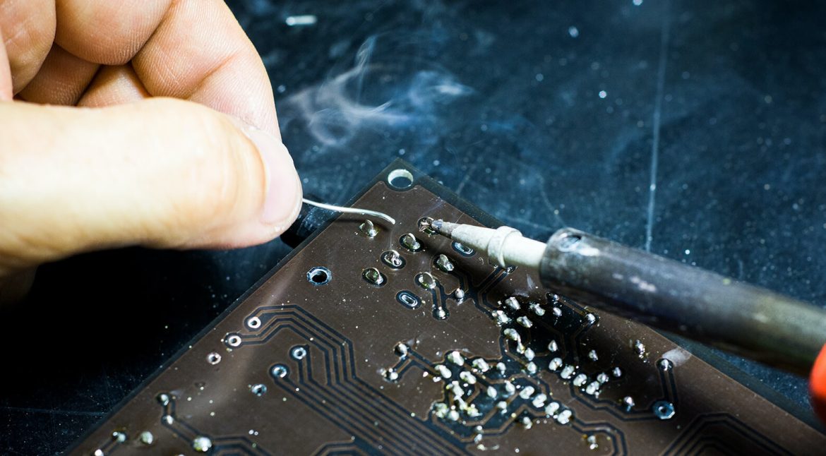
Where the board carries both surface mount and through-hole parts, the flow depends on which side the through-hole parts are on. In the common arrangement the surface mount parts are on the A side and the through-hole parts on the B side: the A side is printed, populated and reflowed, the through-hole parts are inserted, and the joints are made by wave soldering, with hand soldering for small numbers. The alternative is to print, place and reflow the A side, dispense paste onto the through-hole pads, insert the parts and reflow the second side.
Where surface mount parts are on both sides and through-hole parts are also present, the two sides are reflowed first and the through-hole joints are then hand soldered. Each arrangement imposes different constraints on the design. The wave soldered side needs the component orientation and the solder thieves that keep a trailing joint from bridging, while the reflowed side needs thermal relief on any pad connected to a large area of copper.

Cleaning and Inspection
Cleaning removes the flux residue and other material left on the board that could affect its electrical behaviour. Where a no-clean solder is used and the residues are benign, cleaning can be omitted, but low power and high impedance circuits are sensitive to residue in a way that a logic board is not, and the decision should follow the circuit rather than the convenience of the process.
Inspection follows cleaning. Visual inspection confirms that the parts are present, correctly oriented and correctly seated, and it is the check that catches the errors a placement machine cannot detect on its own. Where the board carries parts whose joints cannot be seen, X-ray inspection covers them. Rework closes the sequence: a board with a single defective joint is repaired rather than scrapped, which is only possible if the layout left access for it.
What the Line Needs from the Design
The list of things the assembly process needs from the board is short, and all of it is cheaper to provide in the layout than to work around in production. Pads sized for the component and spaced so that the paste does not bridge. Fiducials, so that the placement machine can find the board. A panel that the machine can handle and that breaks apart without damaging the edges. A component orientation that suits the solder wave, where wave soldering is used. And thermal relief on pads connected to large copper areas, so that the joint can reach soldering temperature.
Two of those interact with the parts themselves. Components that are prone to shifting during reflow, and the reasons they shift, are described in SMT component shift causes. And where the finished assembly will be exposed to moisture, the protective coating applied after assembly is described in conformal coating for board protection.
FAQ
When is a stencil required? When the board carries SOT, SOP, PQFP, PLCC or BGA packages, or chip components of 0805 and below. Where the only surface mount parts are 1206 or larger, paste can be dispensed without one.
Why does the second reflow pass matter? Because the parts fitted on the first pass have to survive it and stay in place when the board is turned over. That is why heavy components are usually placed on the side that is reflowed first.
Can through-hole and surface mount parts share a board? Yes, and the flow depends on which side the through-hole parts are on. The common arrangement reflows the surface mount side first and wave solders the through-hole joints afterwards.
Is cleaning always necessary? No. A no-clean process can omit it where the residue is benign, but low power and high impedance circuits are sensitive to residue and usually justify cleaning.