Solder Mask Opening Over PCB Traces: When and How
Most copper on a finished board is covered by solder mask, and that covering is assumed rather than designed. Occasionally a designer deliberately removes the mask over a trace, and the result is a solder mask opening that exposes bare copper. The technique solves real problems, from adding current capacity to creating a deliberate solder bridge, but it also introduces assembly and corrosion risks that are easy to overlook. Used deliberately and documented properly, it is a useful tool.
What a Solder Mask Opening Actually Exposes
A solder mask opening is simply an area where the mask layer is omitted, so the copper beneath it is bare. It is not a pad unless the copper underneath was designed as one, and it does not change the circuit: the trace is still the same width and the same layer. What changes is the surface, which is now exposed to the plating or coating that the fabricator applies, and to whatever the assembly process brings into contact with it.
This distinction matters during documentation. A mask opening drawn over a narrow signal trace creates a long exposed line that could be bridged accidentally, while the same opening over a wide power trace gives a useful tinning area. The mask layer is a manufacturing drawing as much as an electrical one, and it should be reviewed with that in mind.
Why Expose a Trace: Tinning, Shunt and Heat
The most common reason is to add solder or plating material to a conductor. Opening the mask over a power trace and tinning it during assembly increases the effective cross section, which lowers resistance and helps the trace run cooler. On high current boards this is a cheap alternative to heavier copper, because the extra material is added only where it is needed rather than across the whole layer.
A second reason is to create a deliberate bridge. Where a designer wants two nets joined by solder, or wants a selectable option that can be closed on the production line, an opening over the gap makes that joint reliable and inspectable. A third case is thermal. Exposing copper beside a hot component gives the rework operator a place to attach a thermal shunt, although the benefit is modest compared with a proper copper pour.
Design Rules for Opening Width and Clearance
Treat an opening like a pad for the purpose of clearance. The mask must overlap the copper edge by a margin that the fabricator can register reliably, typically around 0.05 to 0.1 millimetre per side, otherwise mask slivers or exposed copper beyond the intended outline appear. Keep the opening aligned with the trace so that no part of the exposed copper sits closer to a neighbouring net than the normal spacing rules allow.
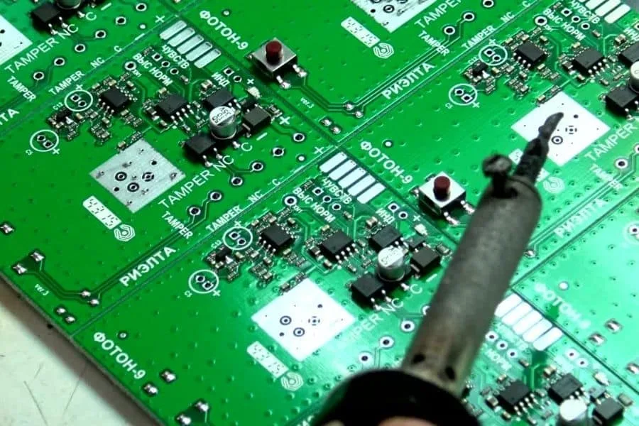
Width matters more than length. A long, narrow exposure is difficult to tin evenly and easy to bridge, while a short exposure of a wide trace is straightforward. Where the opening has to be long, break it into shorter sections with mask between them, which also stops solder from wicking along the whole trace. Designers should also confirm that the copper under the opening really is the trace, since an opening over bare laminate exposes nothing useful.
Assembly Risks: Bridging, Wicking and Corrosion
Trace exposure makes solder wicking the risk that appears first. During reflow, molten solder travels along exposed tinned copper and can carry enough material to create a bridge or to starve a nearby joint. Keep exposure away from fine pitch pin fields, keep it downstream of the solder source rather than upstream, and avoid running an exposed trace between two fine pitch components.
Corrosion is the slow risk. Exposed copper that is only tinned, or that relies on a thin organic coating, will oxidise and can grow dendrites in humid conditions, especially where the coating is damaged during assembly. Where the exposure is permanent rather than a temporary option, specify a surface finish that protects it, which is the same reasoning that governs unintentionally exposed copper elsewhere on the board.
Surface Finish Choices for Open Copper
The finish applied to the board determines how long an opening remains solderable. Hot air solder levelling covers the copper with solder and tolerates handling well. Immersion finishes such as silver, tin or gold give a flatter surface and are kinder to fine geometry. Organic solderability preservatives are the cheapest option, but their protection is limited, so they suit openings that will be consumed during the first assembly pass.

Where the exposure carries current continuously rather than being soldered once, silver or gold finishes are usually preferable, because tin can form whiskers and a purely organic coating does not survive thermal cycling. The choice should be documented with the opening so that the fabricator applies the same finish to the pad and the exposed trace, which is where inconsistencies usually appear.
Documentation and Fabrication Notes
Put the openings on a dedicated mask layer rather than drawing them as copper features, and add a note listing which ones are intentional. Fabricators routinely remove mask slivers and enlarge openings to meet their process, so an opening that is not called out may be adjusted without the designer noticing. A short note explaining the purpose of each opening saves a round of questions during fabrication review.
Where the exposure is used to carry current, state the intended tinning and the expected current so the fabricator can comment on the plating. Our guidance on trace width and current calculation covers how much cross section the added solder actually contributes, which is often less than the designer expects because solder resistivity is far higher than copper.
Inspection and Standards
Inspection should confirm three things: that the opening is where the drawing says, that the copper beneath it is intact and free of nicks, and that the finish covers the exposed area uniformly. Visual inspection is usually enough for wide openings, while a microscope is needed for fine ones where mask slivers or leftover resist are the likely defects.
Standard pad and mask design rules already cover the registration and annulus requirements that apply here, so an opening that follows the same discipline as a pad will normally pass both fabrication and assembly review. Treat any exception as a deliberate deviation with a written reason, and keep the record with the fabrication drawing.
FAQ
Is an opening over a trace the same as a test point? No. A test point is a defined pad with a known size and spacing that a probe is designed to touch. An opening over a trace exposes copper but gives no control over probe position or contact area, and probing it can damage the mask edge. Where the board will be tested, use a real test point.
How much current does tinning actually add? Less than most designers assume. Solder has a resistivity roughly six to ten times that of copper, so a solder layer of similar thickness carries far less current for the same geometry. Tinning helps, mainly by adding cross section and by improving heat spreading, but it does not replace proper trace sizing.
Can I use a mask opening to make a solder jumper? Yes, and it is a common technique. Keep the gap between the two copper areas small enough to be bridged with a normal soldering iron, place the opening on the assembly drawing, and decide in advance whether the joint should be made on every unit or only as a configuration option. Document the choice so it is not missed in production.