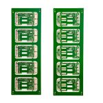
Exposed Copper on a PCB Pad: Causes and Cures
Bare copper is the normal state of a pad before the finish is applied and an abnormal state almost anywhere else. When it appears where it should not, either the mask has failed, the finish has been damaged, or handling has removed a protective layer, and the copper beneath begins to oxidise within hours. The result ranges from a cosmetic complaint to a genuine solderability problem, and the distinction depends on where the copper is and how long it stays that way. This guide covers what causes exposed copper, what it does to assembly, and how to prevent it.
What Counts as Exposed Copper
Copper is meant to be exposed in three places: pads to be soldered, test points and any surface that carries a specified finish. Outside those areas it should be covered by mask. The distinction matters because the two cases behave differently. A pad is exposed deliberately and receives a finish that resists oxidation; a scratch through the mask, a pinhole or an unplanned opening leaves copper with no protection at all.
Some designs blur the line. A ground pad left open for shielding contact, a thermal pad under a package or a mask defined pad on a press fit hole are all deliberate exposures that still need a stated finish. If the fabrication drawing does not say what surface finish belongs on them, the answer may vary from one lot to the next.
How the Mask Fails
A solder mask defect is the most common route to unintended exposure. Pinholes form where the coating is too thin or where a foreign particle sat during lamination; scratches occur during handling, drilling and routing; and poor adhesion at a copper step lets the mask lift along an edge. Registration errors can also leave copper bare where an opening shifted onto a trace rather than onto a pad.
Process condition matters as much as the artwork. Under cured mask stays soft and is easily damaged; over cured mask becomes brittle and cracks along the copper edges. Developing that is too aggressive can thin the coating over fine features, and cleaning that is too harsh can abrade an otherwise sound surface. Each of these produces exposure that only appears after the panel has been through several process steps.
Oxidation and Solderability Risk
Copper oxidises quickly in air, and the oxide layer does not wet with solder. A small exposed area on a non functional surface may never matter; the same area under a pad or along a trace that must be soldered will resist wetting and produce a weak or incomplete joint. Oxide growth accelerates with humidity and temperature, so a board stored in a warm damp warehouse degrades far faster than one kept in a controlled store.
Where a finish is present, oxidation is normally held back. The problem arises when the finish itself is damaged: a scratch through an exposed copper pad finish exposes the base metal underneath and places the two materials side by side. That boundary is where corrosion and poor wetting usually begin, and it is why finish damage should be treated as a functional defect rather than a cosmetic one.

Contamination and Handling Damage
Fingerprints, solder paste residue, flux and airborne contamination all attack an unprotected copper surface. Salts and organic acids in a fingerprint etch the metal slowly and leave a residue that prevents wetting even after cleaning. Where the contaminant contains sulphur or chlorine, the corrosion can continue long after the board has been assembled and can produce leakage currents between fine features.
Handling damage follows from the same causes. Boards stacked without interleaving abrade each other; vacuum pick up tools leave marks; and packing materials that are not sulphur free attack silver and copper surfaces during transport. The controls are unglamorous but effective: gloves, interleaving, a controlled packing specification and a storage area that is dry and free of reactive vapours.
Detection and Inspection
Visual inspection catches large areas of exposed copper, but the small ones need better tools. Automated optical inspection detects colour and reflectivity differences across the panel, which reveals pinholes, scratches and lifted mask that a human eye will miss on a dense board. Where the exposure is on a fine pitch footprint, inspection should be done before assembly rather than relying on the assembly line to find it.
For critical products, a cleanliness and surface analysis check on the first article gives a baseline for ionic contamination and for the state of the finish. That baseline is what makes it possible to tell whether a later batch has drifted, and it turns a subjective argument about discolouration into a measurable one. Our notes on PCB cleaning describe the measurements involved.
Prevention in Design and Process
Design can reduce the opportunity for damage. Avoid very thin mask features, keep openings proportionate to pad size, define the finish on every deliberately exposed area and specify mask clearance so that a small registration shift does not expose a trace. Symmetric stackups and balanced copper reduce the movement that causes openings to land in the wrong place.
Process controls finish the job. Confirm mask cure against the material datasheet, control the handling between mask and finish, and specify packaging that will not react with the surface. On products that will sit in store or travel by sea, add corrosion protection where it does not interfere with soldering; our notes on conformal coating cover the options.
Rework and Repair Limits
Not every exposed area can be repaired. Mask repair compounds exist for small cosmetic defects on non functional surfaces, and they are adequate where the area will not be soldered or handled again. On a pad, however, a repair that changes the surface energy or adds a step in the surface can be worse than the defect it corrects, because it interferes with paste release and joint formation.
The usual rule is to scrap boards with exposure on functional pads and to rework only where the defect lies outside the assembly area. That judgement should be written into the inspection standard rather than left to the operator, because the cost of a masked over defect that later fails in the field is far higher than the cost of the board. Our notes on PCB yield and quality control show how the acceptance criteria are normally structured.
Writing the Finish Requirement Clearly
Most unintended surface problems come back to an ambiguous drawing. State the finish for every exposed area, including the ones that are not soldered, and say whether mask may be printed over a thermal or shielding pad. Add the maximum acceptable defect size on a functional pad, the cleaning requirement before packing and the shelf life the finish is expected to support.
A clear requirement also gives the fabricator a defensible basis for inspection and removes the argument that follows a batch of boards with discoloured copper. Where the design deliberately leaves copper bare for a shielding contact or a thermal interface, note the intended function, because that single line tells the supplier whether an oxide film is a cosmetic inconvenience or a functional failure.
FAQ
Does exposed copper always cause a failure? No. Exposure on a non functional surface may be cosmetic only, but exposure on a pad or a solderable trace risks poor wetting and corrosion, and it should be treated as a functional defect.
Can exposed copper be cleaned and soldered? It can if the oxide is light and the area is properly fluxed, but the process window is narrow. Heavy oxide or contamination usually requires the surface to be reworked or the board to be rejected.
How is exposure prevented during storage? By specifying a finish that resists oxidation, using sulphur free packing materials, keeping the store dry and controlling handling. Shelf life figures assume those conditions are met rather than being optional.