What Is on a Printed Circuit Board: Pads, Vias and Layers
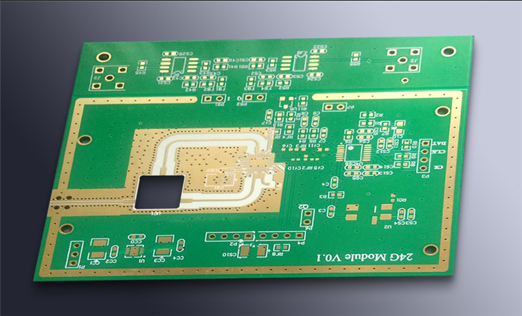
A printed circuit board is a set of copper features carried on an insulating base, organised so that a machine can place parts on it and solder them in one pass. Everything on the board belongs to one of a small number of categories, and knowing which category a feature belongs to explains what it is for.
This article describes the elements that make up a board, the layer structures that are available, and the working layers that appear in the design data but not on the finished product.
The Elements of a Board
The pad is the metal area where a component lead or a solder ball is joined. It is sized around the lead it has to accept and the solder joint it has to form, and its dimensions are set by the component package rather than by the electrical requirements of the net.
Trace geometry follows the pad. A trace is the copper that carries the signal, and its width is chosen from the current it has to carry and the impedance it has to present. Where a trace is wide and close to another, the spacing between them becomes the limiting factor in the design, and the spacing rule is usually the one that decides how densely the board can be routed.
Vias and What They Connect
A via is a plated hole that connects copper on different layers. A through via passes from the top to the bottom and is the simplest to make; a blind via reaches an inner layer from one outer surface, and a buried via connects two inner layers without reaching either surface.
Vias also carry current and heat, and where they are used to move heat away from a device they are placed in an array under the thermal pad. The size of the hole, the size of the pad around it and the plating thickness are all specified by the rules that govern via geometry.
Mounting Holes, Connectors and Fills
A mounting hole is not an electrical feature, and it is often not plated. Its position is fixed by the mechanical drawing and its size by the fastener that will pass through it, and the copper around it has to stand back far enough that the head of the screw cannot touch a trace.
Connectors are the parts that make the board a component of a system, and they are placed at the positions the enclosure requires. Fills are the areas of copper poured on a layer to carry a ground or power connection and to reduce the impedance of the return path. The placement of the outline and its mounting features decides where all of these can be.
The Electrical Boundary
The boundary is the outline within which every component and every copper feature must lie. It is also the line along which the board will be separated from the panel, and because the separation has a tolerance, copper has to keep a distance from it.
A board whose components overhang the boundary will not fit the fixture that holds it during assembly, and one whose copper crosses it will be exposed when the edge is profiled. The boundary is therefore set early, from the mechanical drawing, and treated as a constraint on everything placed afterwards.
Single, Double and Multilayer Constructions
The simplest board has copper on one side only. Components are placed on the bare side and the copper side carries the routing and the solder joints, which suits circuits that can be routed without crossing. It is cheap to make and difficult to route as soon as the circuit has any complexity at all.
A double-sided board has copper on both surfaces, connected by plated through holes. Components can be placed on either side, and the two layers can cross each other without shorting because the connection between them is made only where a via is placed. This is the most common construction for ordinary products. Where more routing channels are needed than two layers can provide, the boards are bonded together into a multilayer stack with inner layers used for signals, power and ground. The general description of what a circuit board is covers the same progression.
Working Layers in the Design Data
A multilayer board adds inner layers, which are used as signal layers, as power and ground planes whose large continuous copper lowers the impedance of the supply, or as a mixture of both. A plane layer is not a solid sheet in practice: it is divided into regions that carry different nets and separated by clearances.
Signal layers hold the traces, and the layers next to a plane are the ones used for nets that need a defined reference. Drill data is not a copper layer at all but a separate description of every hole, its size and its plating, and it is what the drilling machine reads.
Mask, Paste and Silkscreen
The solder mask is the polymer coating that covers the copper except where solder has to reach it. It prevents bridging between adjacent pads, protects the surface between assembly steps and provides electrical insulation on the finished board.
The paste layer is not a coating on the board. It describes the openings in the stencil through which solder paste is printed onto the surface mount pads, and it is used by the assembly house rather than by the fabricator. The silkscreen is the printed legend that carries reference designators, orientation marks and part numbers, and it is the only layer whose purpose is to be read by people.
How the Layers Work Together
The finished board is the result of registering all of these layers to each other. The pads have to line up with the mask openings and the paste apertures, the vias have to land on the pads they connect, and the legend has to sit clear of every opening so that it survives assembly.
Registration tolerance is what makes the design rules necessary. Each layer is produced by a separate operation with its own tolerance, and the design has to leave enough margin that the worst-case combination still produces a working board. That is why a pad is larger than a hole, why a mask opening is larger than a pad, and why copper keeps its distance from the edge. The appearance of the coating is a separate matter, as the notes on solder mask colour and quality explain.
FAQ
How many layers does a board need? As many as the routing and the power distribution require. The count is usually driven by the number of nets that must cross each other and by the need for a continuous reference plane.
Is a plated mounting hole better than a plain one? A plated hole can be connected to a ground net to shield the fastener, and it is stronger in a thin board. Where the hole will be used as a chassis connection, the plating is deliberate.
Why does the paste layer matter to a designer? Because it defines how much solder the assembly receives. A paste aperture that is too large or too small changes the joint, and on fine-pitch parts it changes the risk of bridging.