Solder Mask Orange Peel and Blooming: Causes and Fixes
Orange peel is a fine, regular dimpling of the cured solder mask surface that resembles the skin of a citrus fruit. Blooming is a milky or hazy discolouration that appears after cure and often grows worse with time or with a thermal excursion.
The two are different defects with different causes, but they share a common origin in the way the coating dries and cures. Both are surface phenomena, and both are usually visible in raking light long before they cause a functional failure.
What Orange Peel Looks Like
The defect shows as a uniform pattern of shallow depressions with a spacing of a fraction of a millimetre. Under diffuse light it may be invisible; under a low angle light it becomes obvious because every dimple casts a small shadow.
Because the texture is shallow, it rarely affects electrical performance. Its significance is that it signals that the coating did not flow as intended, and the same conditions that produced it are often marginal for adhesion and coverage over conductor edges.
Why the Surface Does Not Level
A coating levels because surface tension pulls the liquid film flat while it is still fluid. Levelling stops when the viscosity rises enough to freeze the surface profile, and anything that accelerates the rise in viscosity leaves the profile in place.
Solvent loss is the main mechanism. If the solvent flashes off quickly, the surface viscosity rises while the film underneath is still moving, and the result is a skin that cannot reflow. The dimples come from the droplet pattern of the application method or from air movement over the wet film.
Viscosity, Thinners and Flash Off
Ink viscosity is set for the application method and should be measured rather than judged by eye. Adding thinner to make the ink easier to spray lowers the solids content, and a film with less solids shrinks more during drying, which exaggerates any surface texture.
Flash off time matters as much as viscosity. A panel that goes into the oven too quickly traps solvent under a skin, while one that sits too long in a draughty area skins over before the oven. Both cases lock in a surface profile. The correct interval comes from the ink supplier and should be stated in the work instruction in minutes rather than described as a short wait. Air movement is the variable that is easiest to miss: a door left open beside the coating booth will skin the surface of the panels nearest it while leaving the rest of the batch untouched.
Spray, Screen and Curtain Application
Spray application produces the droplet pattern that becomes visible when the film does not level. Nozzle condition, pressure and gun distance all affect droplet size, and a partly blocked nozzle produces a coarse pattern that cannot level out.
Screen printing has a different set of causes. A screen mesh that is too coarse leaves a visible weave pattern, and squeegee pressure that is too high drives ink into the mesh opening rather than laying it flat. Curtain coating tends to give the smoothest surface, provided the curtain is stable and free of bubbles. Film thickness interacts with all of them, because a thin film has less material available to flow and therefore levels more slowly than a thicker one.
Blooming: Appearance and Chemistry
Blooming appears as a white or milky haze rather than a texture. It is most often seen after cure, and it can be traced to incompletely reacted material migrating to the surface, to moisture absorbed during storage, or to a reaction between the coating and a residue on the board.
The defect often appears or worsens after a second thermal excursion, which is the clue that the coating was not fully reacted. Under cure is the usual underlying condition, and it should be investigated with a cure measurement rather than treated as a cosmetic issue.
Drying and Cure Interaction
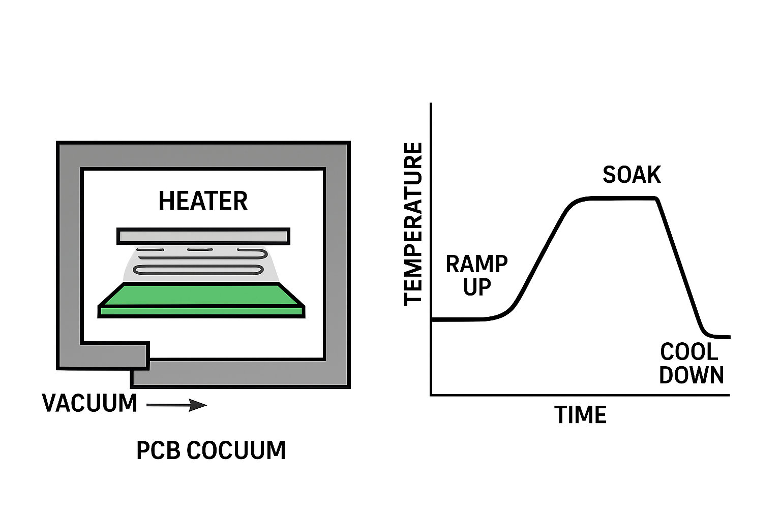
The drying stage removes solvent, and the cure stage completes the crosslinking. If the drying stage is too short, solvent remains under the surface and produces blisters or blooming during cure; if the cure is too cool or too short, the film stays under reacted and the surface remains sensitive to moisture and to flux.
Oven loading is part of the same problem. Panels stacked closely, or placed where the airflow is uneven, will not all reach the same temperature, and the panels that lag will show the defects. The finish quality of the later soldering step is affected when the mask has not cured properly.
Contamination and Substrate Effects
Residue on the copper or on the laminate surface changes the way the coating wets it. Oils from handling, flux residue from a previous operation and salts left by an incomplete rinse all raise the local surface energy difference, which produces craters, fish eyes and hazy patches rather than a uniform film.
The copper topography contributes as well. A very rough copper surface, or one with an oxide layer of uneven thickness, cannot be covered smoothly by a thin film, and the roughness will telegraph through to the surface even if the coating itself is applied correctly. Restoring the copper surface after a repair should therefore be treated as part of the coating process rather than as a separate operation.
Inspection Under the Right Light
Both defects should be inspected with a defined lighting setup. A diffuse source hides orange peel, while a point source at a low angle reveals it. Blooming is best seen against a dark background under diffuse light or with the panel tilted.
A documented inspection setup with a fixed lamp position makes the judgement repeatable between inspectors and shifts. Photographing the boundary sample under that lighting and keeping the image with the work instruction removes the need to describe a texture in words. Where the customer has a limit on surface appearance, a boundary sample that shows the worst acceptable condition removes most of the argument.
Corrective Actions and Records
Correcting orange peel means restoring the film’s ability to level: check the thinner ratio and the solids content, review flash off time, and inspect the application equipment for wear or blockage. Correcting blooming means confirming the cure: check the oven profile, the loading pattern and the cure state of the coating.
Records should include the ink lot, the viscosity measurement, the application parameters, the oven profile and the inspection result. Where a defect appears on one panel of a batch, those fields show whether the process changed or whether one panel was treated differently, and they are the reason the next batch does not repeat it.
FAQ
Does orange peel affect solder mask performance? Usually not electrically, because the texture is shallow. It indicates that the film did not level as intended, which often means coverage over conductor edges and adhesion are also marginal.
What causes solder mask blooming? Incomplete reaction of the coating is the usual cause, sometimes combined with moisture absorbed in storage or residue on the board. It often appears after a second thermal excursion.
How can both defects be prevented? By controlling ink viscosity and solids, keeping a defined flash off interval, verifying the cure profile and ensuring the board enters the coating line free of oils, flux and salt residue.
}