Solder Mask Printing: Process Steps And Controls
Solder mask is applied over the whole panel and then patterned, which means the printing step is only one part of a sequence. Getting it right depends on what happened before the ink touched the board and what happens after it is exposed, and a defect that looks like a printing problem often traces back to the pre-treatment or the cure.
This article describes the steps of solder mask printing, the variables that are controlled at each one, and the defects that appear when a variable drifts.
The process is mature and well understood, which is precisely why the failures tend to be process control failures rather than mysteries.
Pre-Treatment: Preparing The Surface
Ink adheres to whatever it is printed onto, so the surface has to be clean, dry and free of oxide. Pre-treatment usually combines a chemical clean with a mechanical or micro-etch step, followed by a rinse and a dry. The objective is a surface that is uniformly roughened at a microscopic scale, which gives the ink something to grip, without removing so much copper that the trace geometry changes.
The variables are the chemistry concentration, the temperature, the dwell time and the quality of the rinse. An under-treated surface gives poor adhesion, which shows up later as flaking around pads. An over-treated surface can etch the copper enough to affect controlled impedance, so the step has to be measured rather than run by feel. Handling after pre-treatment matters as much, because a fingerprint is enough to create a local adhesion failure.

Ink Selection And Preparation
The ink has to suit the application. A formulation chosen for fine pitch work has different flow and resolution characteristics from one intended for a thick coating over heavy copper, and the colour affects both the exposure energy required and the contrast available for inspection. Ink viscosity is the variable most often adjusted at the press, and it changes with temperature, so a shop that does not control the room temperature is adjusting the same parameter twice.
Thinners are used to bring the viscosity back into range, but they alter the solids content and therefore the cured thickness and the cure behaviour. The reliable practice is to mix the ink to a specified viscosity, to keep the environment stable, and to verify the printed thickness on the product rather than on a test piece from a different part of the panel.
Printing, Coating And Imagining
Printing is the step that puts the ink in place, and it can be done by screen printing, by spray coating or by roller coating. Screen printing pushes the ink through a mesh with a squeegee, and the mesh count, the emulsion thickness, the squeegee angle, the pressure and the speed all affect how much ink is deposited and how evenly. Spray and roller coating deposit a uniform film over the whole panel, which suits thin coatings and fine features, but the film thickness is harder to raise.
After coating, the panel is pre-baked to drive off solvent, exposed through the artwork and developed to wash away the unexposed material. The exposure energy determines how well the pattern is defined and how well the film survives development; too little and the edges are ragged, too much and fine openings are closed. The geometry of the openings is fixed by the design, but whether they come out clean is a process question.
Curing And Its Limits
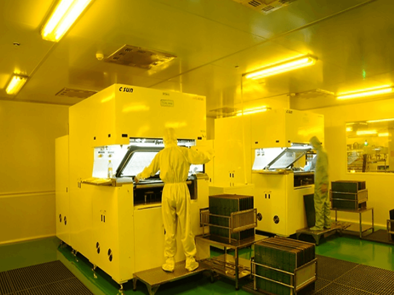
The final cure sets the film’s mechanical strength, its chemical resistance and its colour. Thermal curing in an oven and ultraviolet curing are both used, and some processes combine them so that the film is set by ultraviolet light where it has been exposed and finished by heat. The cure profile has to suit the ink, and it has to be verified on the panel: a film that is under-cured scratches easily and holds flux residues, while one that is over-cured becomes brittle and cracks when the panel is depanelised.
Thickness is linked to the cure as well. A thick film needs more energy to cure through, so a heavy coating printed with a profile set for a thin one will be soft at the bottom. That is why the printed thickness is normally measured and recorded rather than assumed from the process settings.
Inspection And Repair
Inspection after curing covers appearance, thickness and adhesion. Appearance finds the defects that are visible: pinholes, skips, uneven colour, ink on a pad that should be open. Thickness is measured on the cured film. Adhesion is checked by a tape test or a similar method on a coupon, and it is the check that reveals a pre-treatment problem before the boards are assembled.
Repair is possible for small defects using a touch-up ink, and for missing mask over a pad it is usually better to strip and reprint the panel if the quantity justifies it. The judgement depends on where the defect is: a pinhole over a wide trace is cosmetic, while a defect in a mask dam between fine pitch pads is a bridging risk. Recording defects by type and location is what makes the cause visible, and the quality characteristics recorded for the board should include what was found.
Where The Defects Come From
Most mask defects have a specific cause. Pinholes come from contamination or from bubbles in the ink. Uneven thickness comes from the squeegee, the mesh or the panel support. Poor adhesion comes from pre-treatment or from a pre-bake that left the film too dry. Ragged openings come from insufficient exposure. Blisters after soldering come from trapped solvent or absorbed moisture. None of these are ambiguous once the film is examined with the process sequence in mind, and each points to a parameter that can be changed.
Where the mask covers an outer layer trace, its thickness also shifts the impedance slightly, so the coating is part of the electrical specification as well as the protective one. gopcb controls pre-treatment, printing, cure and inspection as one sequence rather than as separate steps, which is what keeps the results repeatable across panels. The same film also interacts with the finish applied after it, and a properly cured mask is what allows the openings to be plated or finished without contamination.
Process Control and Verification
On a design of this kind, curing is the item that decides how the rest of the board is arranged. Where the requirement is not written down, the shop supplies its own default, and the default is chosen for the process rather than for the design. The measurements that matter are the repeatable ones: conductor width and spacing, annular ring, finished hole size, plating thickness and surface finish are all verifiable on a coupon that travels with the panel.
Related reading: our fabrication notes, board quality and design release notes cover the same ground.
FAQ
Why is screen printing still used if spray coating exists? Because it deposits a thicker film reliably, which is what heavy copper and wide pad spacing need. Spray coating suits thin, uniform films over fine features.
How thick should the mask be? It depends on the ink and the feature size. Fine openings need a thinner film to develop cleanly, while heavy copper needs a thicker one to cover the trace edges.
Can a defect in the mask be fixed before assembly? Small cosmetic defects can be touched up. A defect that affects a mask dam between pads should be treated as a reason to reprint rather than to repair.