
Solder Mask Thickness and Coverage over Copper Features
Solder mask is specified by colour in most design packages and by nothing else, yet the two numbers that decide whether it survives assembly are the thickness over copper and the degree of cure. A mask that is thin at the edge of a trace, or that retains solvent because the cure was shortened, passes fabrication inspection and then blisters in the reflow oven. This article covers how thickness varies, how to measure it, and how cure and adhesion are verified.
What Solder Mask Thickness Means
Solder mask thickness is measured over bare laminate on one coupon and over a conductor on another, because the two values differ and both matter. A typical liquid photoimageable mask measures 15 to 25 micrometres over laminate and 8 to 15 micrometres over a 35 micrometre trace, with the reduction caused by flow away from the raised copper during cure.
A class designation takes the lower figure as the controlling value. Where the specification calls for a high thickness, the fabricator has to build it over the trace, not over the laminate, so the coupon used for acceptance must include both.
Why Thickness over Copper Differs
The mask is printed as a liquid or laminated as a film and then flows during the pre-cure, so it drains away from raised features and pools in the gaps between them. The result is a thinner coating over the crest of every trace and a thicker coating in the spaces, which is the opposite of what an even print would suggest.
Trace height makes this worse. On a 70 micrometre copper layer the difference between crest and space is larger, and on heavy copper the mask over the trace can fall below the minimum even when the coupon measured over laminate looks comfortable.
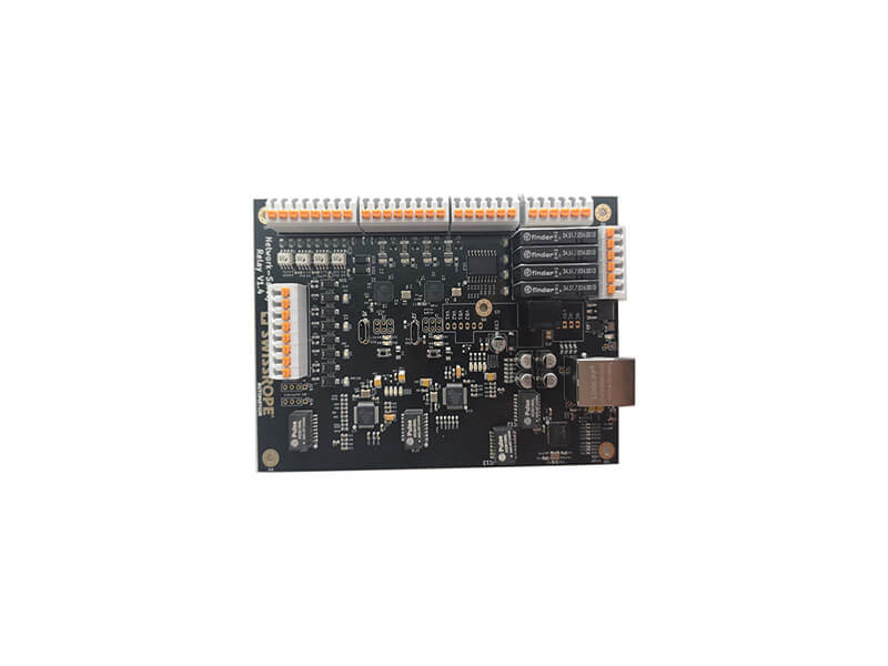
The pattern of a coupon matters for this reason. A coupon with wide open areas will always measure thicker than the same mask over a dense trace pattern.
Measurement Methods
Cross section under a measuring microscope is the reference method, because it shows the mask over a real trace and over laminate in one image and allows both to be measured at the same magnification. The section has to be cut through features the customer cares about rather than through a test area alone.
Non-contact optical or magnetic gauges are used for routine control on coupons, and they are fast enough to run every panel. The two methods have to be correlated once, because a gauge that reads 5 micrometres higher than a section will cause a batch to be accepted that a section would reject.
Cure Window and Solvent Retention
Cure is the variable that a thickness measurement cannot see. A mask that is undercured retains solvent, and the solvent is released as vapour when the assembly passes through reflow, which lifts the mask from the copper in blisters and pockets.
The cure schedule is normally 150 degrees Celsius for about 60 minutes for a thermal cure, with UV cure used for the surface in a dual cure system. Shortening the bake to gain throughput leaves the deeper material uncured, and the effect only appears on the boards that see the longest profile.
Adhesion and the Tape Test
Adhesion is verified with a cross hatch cut and a tape pull, following the method in IPC-TM-650 2.4.28.1, with the tape applied, rolled down and removed at a controlled angle. A mask that lifts from the trace edges has failed even when no full squares come away.
The test belongs after every process change that touches the mask: a new supplier, a new cure oven, or a change in the surface preparation before print. Adhesion that is marginal at fabrication becomes a lifted mask after the thermal shock of a hot air solder levelling or a wave soldering pass.

The tape test is destructive and is run on a coupon or a scrap panel, but the cut pattern should reproduce the trace widths used on the product, because adhesion depends on the edge area as much as on the chemistry.
Pinholes, Skips and Coverage Defects
Coverage defects come from the print rather than from the chemistry: a mask that is too viscous does not fill between fine traces, and one that is too thin runs into the vias. Print speed, squeegee pressure and mesh selection all move the result, and they are set together for a balance between fill and bleed.
Pinholes are best detected optically with the right contrast, and they matter most over a copper feature that will be exposed to flux. A pinhole over a trace lets flux and alloy reach copper that was meant to be protected, and the resulting corrosion appears months later.
Interaction with Assembly Processes
Hot air solder levelling subjects the mask to a thermal shock and to the mechanical action of the air knife, and it is the finish that finds a marginal cure most quickly. Reflow is gentler, but a mask carrying solvent will still blister where the vapour has nowhere to go.
Wave soldering adds flux, and the residue left in a pinhole or beside a lifted edge is difficult to clean and easy to measure later as ionic contamination. The methods used for that measurement are described in our guide to cleanliness measurement.
Effect on Controlled Impedance
Solder mask has a dielectric constant of roughly 3.5 to 4.0, higher than the air it displaces over a microstrip, so covering a trace lowers its impedance by a few ohms. On a tightly toleranced net that shift is part of the design rather than a process variation.
Because coverage over the trace is thinner than coverage over laminate, the effect is not uniform across a pattern, and the field solver should use the as-built thickness rather than the nominal coating. The stack-up values behind this are covered in our laminate material notes.
Drawing Requirements
The drawing should state the mask type and colour, the thickness over both copper and laminate, the cure schedule, the class, and the treatment of vias. Where a controlled impedance net exists, it should say whether the mask is included in the calculation.
It should also state the finish, because the finish decides how much thermal and mechanical load the mask will see. A specification that names the mask and leaves the finish open has not defined the process the mask will actually survive, which is the point of specifying thickness and cure in the first place.
Mask thickness across a dense pattern is verified on a section cut through the narrowest trace pitch in the design, because that is where the coating over copper is thinnest and where a pinhole would expose a conductor.
Where the coating over a trace falls below eight micrometres, the fabricator can build it up with a second print or by moving to a finer mesh, and the choice is confirmed on a coupon before the panel is released.
FAQ
Which thickness is measured for acceptance? The thickness over copper, because that is the lower of the two values and the one that decides whether the mask survives assembly.
Can a thicker mask be specified without changing anything else? Yes, but the print and cure have to be adjusted to deliver it, so the requirement should be discussed with the fabricator rather than added as a note.
Does a tape test prove the mask is fully cured? No. Tape and cross hatch measure adhesion, while cure is confirmed by the solvent retained in the film and by the behaviour of the panel through a reflow profile.