Ultrasonic Transducer PCB: Design, Materials and Applications
What an Ultrasonic Transducer PCB Does
An ultrasonic transducer converts electrical energy into sound and back again. The piezoelectric element does the physical work, but the printed circuit board around it decides how cleanly the signal is delivered and how much of the returning echo survives. A transmit pulse can reach 50 to 300 volts, while the received echo may be only a few microvolts, so the same board has to carry very different signals without letting one corrupt the other. That combination of high voltage pulsing and low level sensing is what makes ultrasonic transducer PCB design its own discipline.
Key Design Requirements
Low loss. The transmission line from the driver to the transducer must not absorb the pulse. Controlled impedance. The trace and the matching network should present the impedance the driver and the transducer expect. Low noise. The receive path needs a quiet ground and physical separation from switching nodes. High voltage isolation. Creepage and clearance must hold the pulse voltage without arcing. Thermal stability. Materials must keep their electrical properties as the board heats up during continuous pulsing. Mechanical stability. The transducer mounting area must stay flat so the acoustic coupling does not change.
Materials and Stack-Up
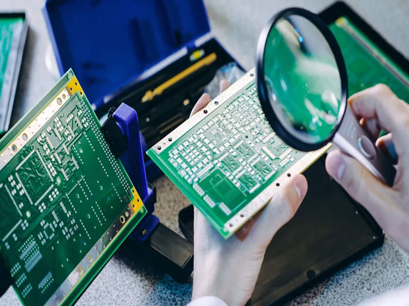
For low frequency ultrasonic designs, in the tens of kilohertz to about one megahertz, a high quality FR4 or a high-Tg laminate is usually enough as long as the loss is low and the thickness is controlled. As the frequency rises into the megahertz range, dielectric loss becomes significant, and low loss laminates with a stable dielectric constant, such as ceramic-filled PTFE or hydrocarbon materials, keep the pulse sharp and the echo strong. A four-layer stack-up with ground planes above and below the sensitive traces is a good default: it shields the receive path, gives a solid reference for the matching network and provides a clean return for the high current transmit loop. Thick copper helps the transmit traces carry the pulse current without heating.
Impedance Matching and Tuning
Piezoelectric transducers are capacitive, so they present a reactive load that the driver cannot match directly. A matching network of series and parallel inductors, sometimes with a resistor for damping, transforms the impedance and tunes the transducer to resonance. On the PCB this network must sit as close to the transducer as possible, with short traces and a solid ground reference, because any added inductance or stray capacitance shifts the resonance. Keeping the driver, the tuning components and the transducer in one compact block, rather than spreading them across the board, is the single most effective layout decision. For multi-element arrays, each channel needs its own matching network and equal trace lengths so that the channels stay in phase.

High Voltage and Isolation
Pulser voltages of 100 volts and above demand attention to creepage and clearance. Keep the high voltage nodes short and away from the low level receive traces, use rounded pads instead of sharp points, and leave generous spacing between the pulse net and any adjacent conductor. Where the pulse path must run near logic, a ground pour between them reduces coupling. Solder mask over the high voltage traces improves the withstand but does not replace distance, so plan the spacing from the start rather than tightening it later.
Grounding, Shielding and Noise
The receive signal is the hardest part. Use a dedicated analog ground for the receive chain and join it to the main ground at a single point to avoid circulating currents. Keep digital switching, clocks and the high current pulse loop out of the analog area, and route the receive traces over an unbroken ground plane. Guard rings around the high impedance input nodes reduce surface leakage, which matters when the board will be coated or used in humid environments. If the transducer is remote, a shielded cable or a driven shield keeps the small signal intact.
Assembly and Reliability
The transducer is usually attached with an adhesive or a mechanical clamp, and the joint has to survive thermal cycling without changing the acoustic path. Conformal coating protects the high impedance nodes from moisture and contamination, but it must be applied consistently, because a coating that wicks onto the transducer face or the matching inductors shifts the tuning. Components in the pulse path should be rated well above the working voltage, and the whole assembly should be tested for gain, bandwidth and noise floor after potting, not before.
Ultrasonic designs live or die on the manufacturing details, so the board has to be built by a partner who understands controlled impedance and clean assembly. Review how PCB manufacturing handles low loss laminates, confirm the analog layout rules in your PCB design and layout, and check the design and manufacturing considerations before release. A prototype PCB assembly run validates the matching network and the noise floor before volume.
Typical Applications
Medical imaging. Probe arrays with many channels and tight phase matching. Non-destructive testing. Flaw detectors and thickness gauges that need a clean echo from a small reflector. Flow and level sensing. Clamp-on flow meters and tank sensors that work through a pipe wall. Automotive. Parking sensors and blind spot detection. Industrial. Cleaning, welding and cutting drivers where the board must survive continuous high power pulsing. Consumer and robotics. Distance measurement and gesture sensing.
FAQ
Can ultrasonic transducers use standard FR4? Yes for low frequency designs. Above roughly one megahertz, low loss laminates keep the pulse and echo much cleaner.
Why is impedance matching so critical? Piezo elements are capacitive, so without matching the driver delivers less energy and the received echo is weaker and noisier.
How much voltage do the traces need to withstand? Many pulser designs run at 100 volts or more, so plan creepage and clearance for the full pulse voltage with margin.
Does conformal coating help? Yes, it stabilises the high impedance nodes, provided it is applied consistently and does not reach the transducer face.
Conclusion
An ultrasonic transducer PCB is a study in contrasts: high voltage pulses on one side, microvolt echoes on the other, and only careful layout keeps them apart. Choose a low loss material, keep the matching network next to the transducer, respect high voltage clearance, give the receive path its own quiet ground, and protect the assembly with a controlled conformal coating. Get those right in 2026 and the board will deliver the sharp pulse and clean echo the application depends on.