PCB Acidic vs Alkaline Etching: Key Differences
What PCB Etching Does
Etching is the step that removes unwanted copper from a printed circuit board and leaves the traces behind. After the pattern is defined by a photoresist or a plated metal resist, the board passes through a chemical bath that dissolves the exposed copper while protecting everything that must stay. Two chemistries dominate the industry: acidic etching and alkaline etching. They remove the same material, but they behave differently, and choosing the wrong one for a given layer or line width leads to undercut, uneven trace width or damaged resists.
Acidic Etching Chemistry
Acidic etchants are based on cupric chloride or ferric chloride, usually with hydrochloric acid and an oxidiser such as hydrogen peroxide. Cupric chloride is the workhorse: as it etches, it regenerates itself, so the bath stays active for a long time and the cost per square metre stays low. Acidic chemistry etches copper quickly and is very tolerant of heavy copper, which makes it the standard choice for inner layers and for boards where a thick copper weight has to be cleared. Its weakness is selectivity: acidic solutions also attack tin and some other metal resists, so it cannot be used after a tin plating step without care.
Alkaline Etching Chemistry
Alkaline etching uses an ammoniacal solution, typically ammonium hydroxide with ammonium chloride, held at a controlled pH and specific gravity. Its key advantage is selectivity. Alkaline etchant dissolves copper but leaves the tin or tin-lead etch resist intact, so it is the natural choice for outer layers, where the pattern is protected by plated tin. It also etches uniformly across the panel and produces a cleaner sidewall on fine lines, which is why high density outer layers with narrow traces rely on it. The trade-off is that the chemistry is more expensive, needs careful pH and copper concentration control, and requires a regeneration or bleed-and-feed system.
Key Differences at a Glance
Chemistry. Acidic uses cupric or ferric chloride; alkaline uses an ammoniacal solution. Resist compatibility. Alkaline is compatible with tin resists, acidic is not. Typical use. Acidic for inner layers and heavy copper, alkaline for plated outer layers. Resolution. Alkaline gives a better etch factor for fine lines. Cost. Acidic chemistry is cheaper and self-regenerating; alkaline costs more but can be regenerated with the right equipment. Control. Alkaline demands tighter pH and density control.

Resolution and Sidewall Quality
Etching is not perfectly vertical. The etchant works sideways as well as down, and the ratio of vertical to lateral attack is the etch factor. A high etch factor means straight sidewalls and predictable trace width. Alkaline etching generally delivers a better etch factor on thin copper, which matters as line widths shrink below 100 microns. Acidic etching is strong on thick copper but tends to undercut more on fine features unless the spray parameters and conveyor speed are tuned carefully. For a board that mixes fine lines and heavy copper, many shops etch heavy layers acidically and fine outer layers alkaline.
Equipment and Process Control
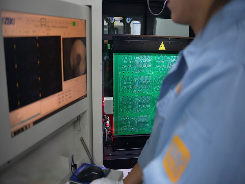
Both chemistries run in conveyorised spray etchers, where nozzles, pressure, temperature and conveyor speed set the dwell time. Acidic lines are simpler to operate and tolerate wider process windows. Alkaline lines need continuous monitoring of pH, copper concentration and specific gravity, and usually a controller that doses ammonia and replenishes the solution automatically. In both cases the critical variables are the same: uniform spray coverage, stable temperature and a dwell time that matches the copper thickness and the required line width.
Cost and Throughput
Acidic etching is the cheaper option on consumables and disposal, and its self-regenerating behaviour keeps the bath productive for a long time, which suits high volume inner layer production. Alkaline etching costs more per litre, but the selective chemistry saves money elsewhere by protecting the tin resist, avoiding extra stripping steps and improving first pass yield on dense outer layers. When you compare the two, compare the total process cost, not the price of the chemicals: rework and scrap on fine lines usually outweigh the etchant difference.
The etching choice has to fit the rest of the fabrication flow. Review how PCB manufacturing sequences inner and outer layer etching, keep trace widths and spacing compatible with the achievable etch factor in your PCB design and layout, and check the design and manufacturing considerations before release. For a new design, a prototype PCB assembly run confirms that the etched line width matches the simulation.
How to Choose
Match the chemistry to the layer and the resist. If you are etching an inner layer before plating, or clearing heavy copper, acidic cupric chloride is the practical choice. If you are etching a plated outer layer protected by tin, alkaline etching is the safe choice because it will not attack the resist. For fine outer layers, prefer alkaline and design lines and spaces the process can hold; for heavy inner layers, prefer acidic and allow for its undercut in your width budget.
FAQ
Which etching process is more accurate? Alkaline etching usually gives a better etch factor on fine lines, while acidic etching handles thick copper better.
Why is alkaline etching used for outer layers? Because it etches copper but leaves the tin plating resist intact, so the pattern is protected during the etch.
Can acidic etching be used after tin plating? Not normally. Acidic solutions attack tin, so they are reserved for inner layers or for plating resists that tolerate acid.
Is alkaline etching more expensive? The chemicals cost more, but regeneration and higher yield on dense layers often offset the difference.
Conclusion
Acidic and alkaline etching remove copper in different ways for different jobs. Acidic cupric chloride is cheap, self-regenerating and strong on heavy copper, which suits inner layers. Alkaline ammoniacal etching is selective to tin resist and cleaner on fine lines, which suits plated outer layers. Choose by layer, resist and line width, keep the etch factor in your width budget, and let the fabricator tune the line so the finished trace matches the design in 2026.