What Is a 6-Layer PCB?
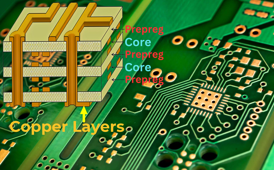
As the name suggests, a 6-Layer PCB contains six conductive copper layers separated by dielectric materials. These layers are interconnected through plated through-holes, blind vias, buried vias, or other interconnection structures to provide electrical connections between components and circuits.
In a typical six-layer board, the top and bottom layers are commonly used as signal layers, while the four internal copper layers can be configured as signal, power, or ground planes depending on the electrical and mechanical requirements of the design.
Compared with four-layer PCBs, six-layer boards provide considerably more routing space and greater flexibility for separating high-speed signals, power distribution, and ground structures. They are therefore well suited for applications requiring better Signal Integrity, electromagnetic compatibility, higher routing density, and more complex power architectures.
Blind and buried vias are also frequently considered in advanced six-layer designs, particularly when the board requires higher interconnection density or HDI structures.
Typical applications include industrial automation and control, robotics, IoT equipment, telecommunications, medical electronics, automotive electronics, test and measurement equipment, aerospace systems, and other sophisticated electronic products.
Why Choose a 6-Layer PCB?
The decision to use a 6-Layer PCB instead of a four- or eight-layer board is usually based on a combination of routing requirements, electrical performance, cost, and product complexity.
Common reasons include:
- A four-layer PCB does not provide enough routing space for the required circuit.
- Better EMC performance is required than a conventional four-layer board can provide.
- The design contains multiple high-speed interfaces with potential crosstalk problems.
- Several power rails or voltage domains must be distributed independently.
- The project requires additional ground or power planes.
- The budget does not justify moving to an eight-layer PCB.
- An eight-layer design would introduce unnecessary complexity for the application.
- Additional layers are needed to improve return-path control and Signal Integrity.
A well-designed six-layer board can provide an effective balance between electrical performance, routing capacity, manufacturing complexity, and cost.
For many products, it represents a practical middle ground between the limitations of a four-layer PCB and the higher cost of an eight-layer design.
Advantages of a 6-Layer PCB
A 6-Layer PCB provides several advantages for complex and high-performance electronic systems.
Improved Signal Integrity
A properly designed six-layer stackup can provide dedicated reference planes close to high-speed signal layers. This creates shorter and more predictable return paths, which can significantly improve Signal Integrity.
A suitable stackup can also reduce loop area, impedance discontinuities, crosstalk, and unwanted electromagnetic radiation.
Better EMC Performance
Additional ground planes provide improved shielding between signal and power structures.
By placing sensitive signal layers next to solid ground reference planes, designers can better control current return paths and reduce electromagnetic coupling. This makes six-layer boards particularly useful when strict EMC requirements apply.
Support for Advanced PCB Technologies
Many advanced PCB technologies can be implemented more effectively when additional layers are available.
For example, HDI PCB structures, controlled impedance routing, blind vias, buried vias, fine-pitch components, and high-density routing can all benefit from the additional design space offered by a six-layer structure.
Higher Component Density
Additional internal routing layers reduce the amount of routing that must be placed on the component layers.
This allows more freedom for placing components on the top and bottom surfaces while using the internal layers for signal routing and power distribution.
When combined with HDI PCB technology, a six-layer board can support significantly higher component and interconnection density.
Flexible Layer Configuration
One of the most important advantages of a six-layer board is its stackup flexibility.
Designers can select different combinations of signal, ground, and power layers according to the requirements of the product. Core and prepreg materials can also be selected to achieve the required dielectric thickness, impedance, thermal performance, and manufacturing cost.
Disadvantages of a 6-Layer PCB
Although six-layer boards offer significant electrical and routing advantages, they also introduce additional cost and manufacturing complexity.
Higher Manufacturing Cost
A six-layer PCB requires more copper, dielectric materials, lamination processes, drilling operations, plating steps, and inspection than a simpler multilayer board.
The cost can increase further when the design requires controlled impedance, fine-line routing, HDI structures, blind or buried vias, special materials, or advanced surface finishes.
More Complex Design
Designing a six-layer board requires careful consideration of layer assignment, signal-return paths, power distribution, impedance, thermal management, and manufacturability.
A poorly designed stackup can waste the additional layers and may even result in worse EMC or signal performance than a properly optimized four-layer design.
More Difficult Debugging
With six conductive layers, many signal paths and power structures are located internally.
Troubleshooting therefore becomes more difficult because internal traces cannot be visually inspected as easily as traces on the outer layers. Designers may need X-ray inspection, electrical testing, simulation, or other diagnostic methods during development and production.
Common 6-Layer PCB Stackups
The 6-Layer PCB Stackup determines how signal, power, and ground layers interact electrically and mechanically.
A typical six-layer PCB contains six copper layers separated by dielectric materials. The dielectric structure may include core materials and prepreg.
The following configurations are commonly considered for different applications.
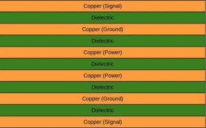
SIG – GND – PWR – PWR – GND – SIG
This is a symmetrical PCB Stackup with signal layers on the outer surfaces and dedicated ground and power planes internally.
The ground layers provide stable reference planes for the outer signal layers, while the two internal power layers can support different voltage domains.
This configuration can work well for high-speed digital systems where multiple power rails are required.
The symmetrical construction can also provide good mechanical stability during lamination and thermal cycling.
SIG – GND – PWR – GND – SIG – GND
This configuration emphasizes ground-plane coverage and electromagnetic shielding.
The internal signal layer is positioned between ground layers, providing strong isolation from adjacent power structures.
This can be advantageous for designs with sensitive signals or demanding EMC requirements.
However, the bottom ground layer can reduce the available component-placement area on the bottom side. Therefore, designers should determine component placement and routing requirements before selecting this configuration.
SIG – PWR – SIG – SIG – GND – SIG
This is a relatively straightforward six-layer arrangement that provides several signal layers.
Although it offers substantial routing capacity, it does not provide the same degree of reference-plane shielding as stackups with dedicated ground planes adjacent to each signal layer.
For high-speed or EMI-sensitive applications, this configuration may therefore require additional analysis and careful routing.
It can be more appropriate for lower-speed systems or designs where EMC and impedance requirements are less demanding.
SIG – GND – PWR – SIG – GND – SIG
This is a more balanced configuration that provides ground reference planes for multiple signal layers.
The top signal layer has a nearby ground reference, while the internal signal layer is also associated with a ground plane. This helps improve return-path control and impedance predictability.
For high-speed designs with a relatively high I/O count, this configuration can provide a good balance between routing capacity and EMC performance.
How to Choose the Right 6-Layer PCB Stackup
There is no single stackup that is suitable for every six-layer PCB.
The optimal 6-Layer PCB Stackup depends on:
- Signal speed and rise time
- Controlled impedance requirements
- Number of power rails
- Number of high-speed interfaces
- EMI sensitivity
- Component density
- Thermal requirements
- Layer-to-layer dielectric thickness
- Manufacturing capabilities
- PCB material
- Overall project budget
High-speed signals should generally be routed close to a continuous reference plane. Designers should also avoid unnecessary plane splits beneath high-speed traces because they can interrupt the return-current path and create impedance discontinuities.
For particularly sensitive interfaces, differential-pair routing, length matching, controlled impedance, via optimization, and appropriate ground stitching should also be considered.
Key Considerations for 6-Layer PCB Design
The flexibility of a 6-Layer PCB must be used intelligently. Adding layers alone does not automatically improve PCB performance.
Layer Arrangement
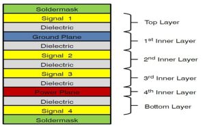
Power and ground planes play a critical role in power distribution, shielding, and return-path control.
A solid ground plane beneath high-speed signal layers can provide a low-inductance return path and help control electromagnetic radiation.
Sensitive signals can also be routed on internal layers between ground references when additional shielding is required.
High-Speed Signal Routing
High-speed signals should be routed with careful attention to their reference planes.
Important practices include:
- Maintain a continuous reference plane beneath high-speed traces.
- Minimize unnecessary vias.
- Keep differential pairs properly coupled.
- Control trace width and spacing.
- Match critical signal lengths when required.
- Avoid abrupt impedance changes.
- Minimize stubs on high-speed nets.
- Keep noisy signals away from sensitive analog or RF circuits.
Using the top and bottom layers for selected high-speed interfaces can provide convenient access to components, while internal signal layers can be used for less critical routing.
Power Integrity
Modern electronic systems often use multiple voltage rails.
Dedicated power planes or carefully designed power regions can reduce power distribution impedance and improve power integrity. Adequate decoupling capacitors should also be placed close to the power pins of high-speed ICs.
The power and ground structure should be considered together with the signal-return path rather than treated as separate design problems.
Thermal Management
Component density and power consumption are often higher in six-layer designs.
Thermal management should therefore be considered from the beginning of the design process.
Designers can use copper planes, thermal vias, larger copper areas, heat sinks, and suitable PCB materials to improve heat dissipation.
Increasing copper thickness can also improve current-carrying capacity and thermal performance, although it may affect fine-line manufacturing and overall cost.
Core and Prepreg Selection
A six-layer board typically contains multiple dielectric layers formed from core materials and prepreg.
The dielectric thickness and electrical properties directly affect impedance calculations.
Important material parameters include:
- Dielectric constant (Dk)
- Dissipation factor (Df)
- CTE
- Thermal conductivity
- Glass transition temperature (Tg)
- Moisture resistance
- Copper compatibility
For high-speed applications, selecting a suitable low-loss dielectric system may be necessary to reduce transmission loss and maintain reliable Signal Integrity.
6-Layer PCB Manufacturing Process
Reliable PCB Manufacturing requires precise control of materials, registration, drilling, plating, etching, lamination, and inspection.
A typical six-layer manufacturing workflow includes:
- Material preparation and inner-layer imaging
- Inner-layer etching
- Automated optical inspection
- Layup and lamination
- Through-hole and microvia drilling
- Desmear and hole-wall preparation
- Electroless copper deposition
- Copper electroplating
- Outer-layer imaging and etching
- Solder mask application
- Surface finishing
- Electrical testing
- Final inspection and quality verification
For advanced boards, manufacturing tolerances must be evaluated during the design stage. A design that exceeds the manufacturer’s actual process capability can result in low yield, higher costs, and longer production cycles.
Therefore, DFM analysis should be performed before production begins.
6-Layer PCB Applications
Because of its balance between performance and cost, the 6-Layer PCB is widely used in applications requiring moderate to high circuit density.
Typical applications include:
- Industrial automation and control
- Robotics
- IoT gateways and devices
- Telecommunications equipment
- Network switches and routers
- Medical equipment
- Automotive electronics
- Test and measurement equipment
- Aerospace electronics
- Industrial computers
- Embedded systems
- Consumer electronics
- High-speed digital equipment
The exact layer configuration should be selected according to the electrical requirements of the application rather than simply following a standard stackup.
Why Choose Kingda for 6-Layer PCB Manufacturing?
Selecting an experienced supplier is important when manufacturing an advanced multilayer PCB.
For six-layer boards, manufacturers must maintain consistent control over multilayer registration, copper thickness, dielectric thickness, drilling, plating, impedance, and final inspection.
Kingda provides PCB manufacturing solutions for projects requiring multilayer structures and demanding electrical performance. Our engineering approach focuses on matching the PCB design with realistic manufacturing capabilities while considering signal integrity, EMC, thermal performance, reliability, and production cost.
When selecting a PCB Manufacturing partner, customers should evaluate:
- Multilayer PCB manufacturing experience
- Fine-line and high-density fabrication capabilities
- Controlled impedance capability
- Reliable layer registration
- Stable drilling and plating processes
- Comprehensive electrical testing
- DFM engineering support
- Consistent quality control
- Responsive technical communication
- Flexible prototype and production support
For projects involving high-speed signals, complex power systems, or demanding EMC requirements, Kingda can help evaluate the layer structure and manufacturing requirements before production.
Conclusion
A 6-Layer PCB provides a practical balance between routing capacity, electrical performance, EMC control, manufacturing complexity, and cost.
The most important factor is not simply the number of layers but how those layers are arranged. A carefully engineered 6-Layer PCB Stackup can provide stable reference planes, controlled impedance, improved Signal Integrity, better power distribution, and stronger EMC performance.
For high-density applications, technologies such as HDI PCB structures, blind and buried vias, fine-line routing, and advanced materials can further improve design flexibility.
By selecting the appropriate stackup, materials, routing strategy, thermal structure, and PCB Manufacturing process, designers can achieve a reliable six-layer PCB that meets both electrical and mechanical requirements.
Kingda can support customers from PCB design evaluation through manufacturing, helping optimize six-layer PCB structures for performance, reliability, manufacturability, and cost.