What Is a Heavy Copper PCB?
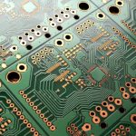
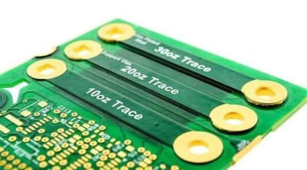
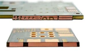
As the name suggests, a Heavy Copper PCB is a printed circuit board manufactured with significantly thicker copper than a standard PCB. In conventional PCB products, copper thickness is commonly around 0.5 to 2 oz, equivalent to approximately 17.5 to 70 μm. When the finished copper thickness exceeds 2 oz (70 μm), the board is generally referred to as a heavy copper PCB. Depending on the copper thickness and application, it may also be described as an Ultra-Heavy Copper PCB.
As electronic systems continue to demand higher power density, reliability, thermal performance, and current-carrying capability, heavy copper technology is becoming increasingly important. These PCBs are widely used in industrial equipment, automotive electronics, power electronics, renewable energy systems, transportation, medical equipment, telecommunications, and aerospace applications.
The required copper thickness varies according to the electrical and thermal requirements of the application. A heavier copper layer can provide a larger current-carrying capacity, stronger mechanical connections, and improved heat dissipation.
Heavy copper PCBs are most commonly manufactured using FR-4 materials. Depending on the application, however, polyimide, aluminum-based, and copper-based substrates can also be used. Polyimide versions are often used to produce heavy copper flexible circuits, while metal-core structures are suitable for applications requiring enhanced thermal management.
What Are the Main Advantages of Heavy Copper PCBs?
The growing use of Heavy Copper Circuit Board technology is closely related to the increasing performance requirements of modern electronics. Many applications require high current, high power density, excellent thermal management, mechanical durability, and long-term reliability.
Compared with standard copper PCBs, heavy copper designs can offer several important advantages.
Higher Current-Carrying Capability
One of the most important benefits of a High-Current PCB is its ability to handle substantially higher current through appropriately designed copper traces and planes.
Increasing copper thickness reduces the electrical resistance of the conductor and allows more current to pass through the PCB without excessive temperature rise. This makes heavy copper particularly suitable for power distribution, motor control, battery systems, power converters, industrial equipment, and electric vehicles.
However, current capacity is not determined by copper thickness alone. Trace width, allowable temperature rise, ambient conditions, copper distribution, and thermal management must also be considered during PCB design.
Improved Thermal Performance
Thicker copper provides a larger thermal conduction path and can help distribute heat away from high-power components.
In high-power applications, heavy copper layers can work together with thermal vias, copper planes, heat sinks, and metal-core substrates to improve overall thermal management.
Higher Mechanical Strength
Thicker copper conductors and plated through-holes generally provide greater mechanical robustness than conventional thin-copper structures.
This can be particularly valuable in automotive, industrial, transportation, aerospace, and other applications where PCBs may experience vibration, thermal cycling, mechanical stress, or long operating periods.
Better Long-Term Reliability
A properly designed heavy copper PCB can provide excellent electrical and mechanical reliability in demanding environments. The increased conductor cross-section helps reduce resistive losses and thermal stress, while robust copper structures can improve the durability of electrical connections.
For high-power equipment where PCB failure could lead to significant downtime or safety concerns, the additional reliability can be a major advantage.
Suitable for Harsh Environments
Heavy copper PCBs can be designed for demanding thermal and mechanical environments. When the correct substrate, surface finish, solder mask, plating process, and protective measures are selected, they can be used in applications exposed to temperature fluctuations, humidity, vibration, and corrosive operating conditions.
It is important to note that environmental resistance depends on the complete PCB material and manufacturing system rather than copper thickness alone.
Heavy Copper PCB Applications
The applications of Heavy Copper PCB technology continue to expand as electronic equipment becomes more powerful and compact.
Common applications include:
- Solar inverters and renewable energy systems
- Battery management and energy storage systems
- Electric and hybrid vehicle power electronics
- Railway traction systems
- Industrial motor controllers
- UPS systems
- Welding equipment
- Power supply systems
- Protection relays
- Torque control systems
- Safety and signaling systems
- Industrial automation equipment
- Medical electronic equipment
- Telecommunications and network power systems
- Aerospace and defense electronics
- High-power switching equipment
- Nuclear and other demanding industrial systems
In automotive and industrial applications, heavy copper PCBs are particularly useful for power modules that must continuously carry high currents while maintaining controlled operating temperatures.
Heavy Copper PCB Capabilities
Kingda provides Heavy Copper PCB Manufacturing solutions for applications requiring high current capacity, thermal performance, and mechanical reliability.
| Capability | Specification |
|---|---|
| Copper Thickness | 2–40 oz |
| Layer Count | 1–12 layers |
| Maximum PCB Size | Up to 24 × 48 in |
| Materials | FR-4, Polyimide, Aluminum Base, Copper Base |
| Board Thickness | 0.5–10.0 mm |
| Special Technologies | Countersunk Holes, Cavity Structures |
| Blind/Buried Vias | Available |
| Minimum Line Width/Spacing | 6 mil (0.15 mm) |
| Minimum Drilled Hole | 8 mil (0.20 mm) |
| Surface Finishes | HASL, ENIG, Immersion Silver, Immersion Tin, ENEPIG, OSP |
| Profiling Methods | V-Cut, Punching, Routing |
| Typical Lead Time | 1–4 weeks |
Actual manufacturing capability depends on copper thickness, layer count, board size, material selection, aspect ratio, and the overall stack-up.
Advantages and Disadvantages of Heavy Copper PCBs
Like other PCB technologies, heavy copper construction has both advantages and limitations. Understanding these factors is important before selecting a heavy copper solution.
Advantages of Heavy Copper PCBs
1. Higher Current Capacity
The greater cross-sectional area of thick copper allows a PCB to carry more current than a conventional thin-copper design when the trace geometry and thermal conditions are properly engineered.
For example, power electronics used in electric vehicles, industrial machinery, battery systems, and large power supplies may require copper weights of 4 oz, 6 oz, 10 oz, or even higher.
In these applications, standard copper thickness may not provide sufficient current-carrying capacity or thermal performance.
2. Excellent Reliability
Standard PCBs often use copper thicknesses of approximately 0.5–1 oz, while heavy copper structures can exceed 2 oz. The thicker copper structure can provide improved current handling and mechanical strength.
Heavy copper is therefore well suited to applications requiring long operating life and high reliability, including automotive power electronics, industrial control systems, medical equipment, and energy systems.
3. Improved Heat Dissipation
Copper has excellent thermal conductivity. Increasing copper thickness can improve the ability of the PCB to spread heat across larger areas.
For high-power components, copper planes and heavy copper structures can be combined with thermal vias, heat sinks, and other thermal solutions to reduce localized temperature rise.
4. Longer Service Life
When properly designed and manufactured, heavy copper PCBs can reduce electrical and thermal stresses within power circuits. This can contribute to longer service life and improved overall system reliability.
The actual service life still depends on the substrate, operating temperature, current load, thermal cycling, assembly process, and environmental conditions.
Disadvantages of Heavy Copper PCBs
1. More Difficult for Fine-Pitch, High-Density Routing
One of the main limitations of heavy copper technology is the difficulty of combining very thick copper with extremely fine traces and spaces.
As copper thickness increases, the etching process becomes more challenging. Excessive lateral etching can affect trace geometry and make it difficult to maintain fine line widths and tight spacing.
Therefore, heavy copper designs are often optimized for power distribution and high-current circuits rather than extremely dense fine-pitch routing.
However, this does not mean heavy copper PCBs cannot contain signal circuitry. Hybrid designs can combine heavy copper power sections with conventional copper signal layers when the stack-up and manufacturing process are carefully engineered.
2. More Complex PCB Manufacturing
Heavy Copper PCB Manufacturing requires tighter process control than standard PCB fabrication.
The etching process becomes more difficult as copper thickness increases because more copper must be removed from unwanted areas. Plating thickness, etching compensation, line geometry, drilling, lamination, and solder mask processing also require careful control.
Lamination is another important challenge. After etching, large copper features can create significant differences in surface topology. The resin system must adequately fill the spaces between copper features to prevent voids, delamination, or other structural defects.
Solder mask application can also become more demanding because heavy copper features may create larger height differences across the PCB surface.
3. Higher Manufacturing Cost
Heavy copper PCBs generally cost more than standard PCBs because they require more copper and may require longer processing times and specialized manufacturing controls.
The cost increase becomes more significant as copper thickness rises. Boards using 4 oz copper or higher can require additional processing, specialized etching and plating parameters, more stringent inspection, and longer production cycles.
Therefore, copper thickness should be selected based on actual electrical and thermal requirements rather than simply choosing the thickest possible copper.
Heavy Copper PCB Design Guidelines
Proper PCB Design is essential for achieving reliable performance in a heavy copper board.
The following guidelines can be used as general design references:
- For heavy copper applications, trace width should generally be selected according to current requirements, copper thickness, and allowable temperature rise.
- A minimum trace width of approximately 0.3 mm may be appropriate for some designs, but the actual value should be confirmed according to the manufacturing process.
- Maintain sufficient clearance between adjacent conductors to accommodate etching tolerances and electrical requirements.
- Copper around mounting holes should maintain adequate clearance from the hole edge.
- High-power components should have sufficient spacing from heat-sensitive components such as large electrolytic capacitors.
- Maintain an appropriate distance between copper features and the PCB edge.
- Use sufficiently wide power and ground conductors.
- Consider thermal vias or copper heat-spreading structures beneath high-power components.
- Avoid unnecessarily high-density routing in areas containing very thick copper.
- Consider current distribution when designing copper planes.
- Ensure the PCB stack-up provides sufficient dielectric thickness for the required voltage and isolation.
- Verify creepage and clearance requirements for high-voltage circuits.
- Confirm that heavy copper areas are compatible with the intended soldering and assembly process.
Thermal Design Considerations
Thermal management is particularly important for high-current PCBs.
Designers should evaluate:
- Copper thickness
- Trace width
- Copper plane area
- Component power dissipation
- Thermal vias
- Heat sinks
- Airflow
- Substrate thermal conductivity
- Ambient temperature
- Maximum allowable temperature rise
A heavy copper layer can improve heat spreading, but it should not be considered a substitute for a complete thermal design.
Advanced Materials for Heavy Copper PCBs
Material selection can significantly affect the performance and manufacturability of a heavy copper PCB.
RTF Copper Foil
Reverse-treated copper foil can provide a suitable surface structure for certain high-performance PCB manufacturing processes. Copper foil selection should consider adhesion, surface roughness, signal requirements, plating compatibility, and manufacturing reliability.
Improved Resin Filling Materials
Heavy copper structures can create substantial differences in surface height during lamination. Resin systems with appropriate flow and filling characteristics can help fill spaces around thick copper features and reduce the risk of voids and delamination.
High-Thermal-Conductivity Substrates
For high-power applications, high-thermal-conductivity substrates can improve heat transfer from components into the PCB structure.
Depending on the application, designers may consider conventional FR-4 systems, high-Tg materials, polyimide, aluminum-based substrates, copper-based substrates, or other specialized materials.
Heavy Copper PCB Manufacturing Process
Producing a reliable heavy copper board requires close coordination between PCB design and manufacturing.
A typical process may include:
- Material preparation
- Inner-layer imaging and etching
- Layer alignment
- Lamination
- Mechanical drilling
- Copper plating
- Outer-layer imaging
- Heavy copper plating and etching
- Solder mask application
- Surface finishing
- Electrical testing
- Automated optical inspection
- Final dimensional inspection
- Packaging and shipment
For very thick copper, manufacturing parameters must be adjusted according to the actual copper weight and board construction.
Process control is especially important for plating thickness, etching accuracy, hole quality, resin filling, solder mask coverage, and surface flatness.
Why Choose Kingda for Heavy Copper PCB Manufacturing?
As demand for high-power, high-reliability electronics continues to increase, heavy copper technology has become an important solution for power distribution, thermal management, and high-current applications.
Kingda supports customers requiring Heavy Copper Circuit Board solutions for demanding applications. Our manufacturing approach focuses on process control, material selection, copper thickness management, drilling, plating, lamination, inspection, and electrical testing.
Whether the application requires a conventional heavy copper PCB or an Ultra-Heavy Copper PCB, the design should be evaluated according to current requirements, thermal performance, mechanical requirements, manufacturing capability, and overall cost.
With appropriate engineering collaboration, Heavy Copper PCB Manufacturing can provide a reliable solution for power electronics, automotive systems, renewable energy, industrial equipment, transportation, medical devices, and other high-performance electronic products.
Conclusion
A Heavy Copper PCB is designed for applications where standard copper thickness cannot provide sufficient current-carrying capacity, thermal performance, or mechanical robustness. With copper thickness typically exceeding 2 oz, heavy copper technology can support demanding power and high-current applications.
At the same time, thicker copper introduces manufacturing challenges, including etching, lamination, plating, solder mask application, and fine-line routing. Therefore, successful heavy copper PCB production requires careful PCB Design, appropriate materials, advanced manufacturing processes, and strict quality control.
By selecting the correct Copper Thickness and working with an experienced manufacturer, engineers can achieve a balance between electrical performance, thermal management, reliability, manufacturability, and cost.