
What Is Solder Mask And What Does It Do?
Solder mask is the coloured layer that covers most of a finished circuit board, and because it is so familiar it is often taken for granted. It is a polymer coating applied over the copper and the laminate, with openings where the board has to be soldered or connected, and it does several jobs that matter to both the assembly process and the life of the product.
This article explains what solder mask is, what it is for, how the different types and colours relate to the process, and what it does not do.
One point is worth stating at the outset, because it causes confusion: solder mask is not a conformal coating. The two are applied at different stages for different reasons, and one does not substitute for the other.
What The Layer Actually Is
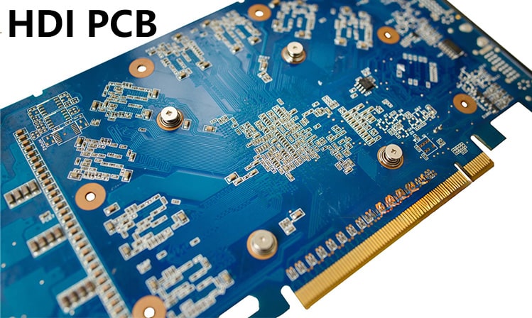
Solder mask is a screen printed or photoimageable polymer, cured onto the board after the copper has been patterned and the surface finish applied. The artwork used to create it is a negative, which is the source of a common misunderstanding. The shapes drawn on the mask layer are the places where the mask will not be present, so the drawing represents the openings rather than the coverage.
In practice the layer exists to separate two things: the areas of copper that should be soldered, and everything else. Around each pad the mask stops short, leaving a small margin. Between adjacent pads it forms a dam, which is the barrier that keeps molten solder from running across the surface and joining two joints together.
The Jobs It Does
The first job is to prevent oxidation. Bare copper oxidises in air, and an oxidised surface is difficult to solder, so the mask covers everything that does not need to be soldered and keeps it in the state the fabricator left it. The second job is to prevent a solder bridge. Where pads are close together, the mask dam between them is what stops the solder from forming an unintended connection, and without it a fine pitch device would be impossible to assemble reliably.
The third job is electrical. The mask is an insulator, and it raises the insulation resistance between adjacent conductors and between a conductor and the environment. That matters both for the working voltage of the board and for its behaviour in humid conditions, where a contaminated surface without a mask can develop leakage paths. The fourth job is mechanical: the mask protects the copper and the laminate from handling damage and from the abrasion of assembly and service.
Types, Colours And Thickness
Liquid photoimageable mask is the standard for most boards. It is applied across the panel, dried, exposed through a film and developed, which gives good resolution and allows small openings. Dry film mask is used where a thicker layer is wanted. The colour is mostly a matter of convention and inspection: green became standard partly because it gives good contrast for automatic optical inspection, and because the chemistry was available first. Black, blue, red, white and matte finishes are all used, and some of them cost more because of the pigment or the inspection difficulty.
The thickness of the mask is small, but it is not zero, and on an outer layer trace it slightly lowers the impedance by changing the dielectric environment above the copper. Where the impedance is being controlled tightly, that effect is included in the calculation, which is one reason the geometry of pad and mask openings is specified rather than left to the process default.
Tenting, Dams And Openings
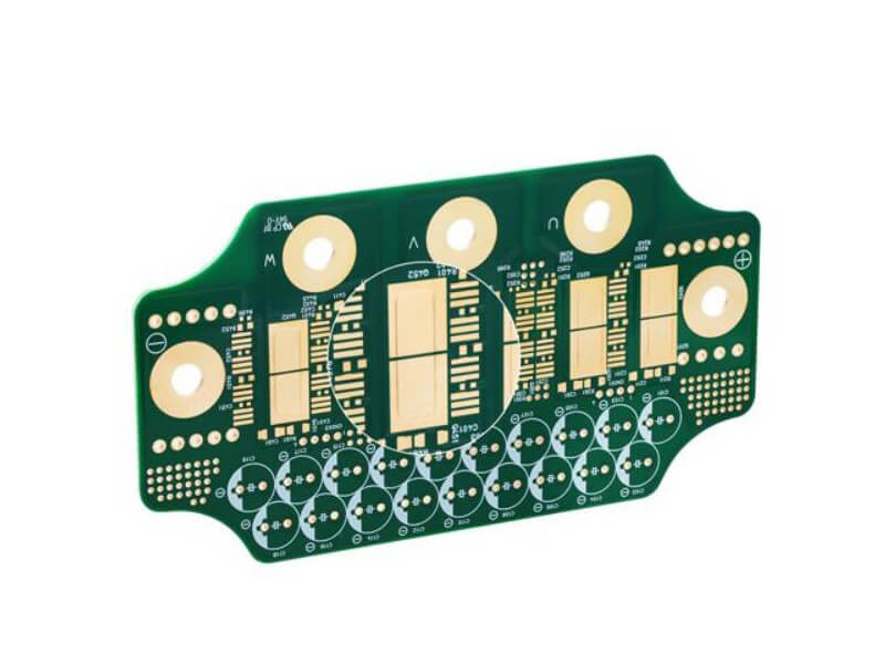
Tenting is the practice of covering a via completely with mask rather than leaving it open. It protects the via from solder and contamination and is normal on ordinary vias. It is not appropriate where the via has to be probed, where it carries a test point, or where the via is in a pad that has to be soldered. Those cases need the mask to open, and the opening has to be specified.
The dam between two openings is a design feature as much as a process one. A dam can only be formed if there is enough space, so the pad spacing and the mask margin together decide whether one is possible. Where the openings merge, the solder has a path between the pads. The remedy is usually a change to the pad geometry or the component choice rather than a change to the mask process.
How The Layer Is Applied And Cured
The mask is coated over the whole panel and then patterned rather than printed in place. The sequence begins with surface preparation, which gives the polymer a clean oxide free surface to bond to, and continues with the coating itself, a pre-bake that drives off solvent, an exposure through the artwork, a development step that washes away the unexposed material, and a final thermal cure that sets the film.
Every one of those steps influences the result. Incomplete preparation is the usual cause of poor adhesion, an incomplete pre-bake traps solvent that later blisters, and a cure that is short or too cool leaves the film soft and chemically weak. Thickness and resolution are also linked: a thick film over a fine opening is difficult to develop cleanly, which is why very small openings may need a thinner coating than the process would otherwise use.
What Solder Mask Is Not
The mask is not a moisture barrier. It is thin, it is not continuous over the whole assembly, and it does not cover the joints or the component bodies. Where a board has to survive humidity, condensation or a corrosive atmosphere, the protection comes from a conformal coating applied over the finished assembly, which is a separate step performed after soldering.
It is also not a substitute for good practice in the layout. A mask opening that is too large leaves copper exposed where it is not wanted; one that is too small risks covering a pad that has to be soldered. Both are decisions in the design data, and both are checked as part of the quality characteristics of the board before it is released for production.
Summary
Solder mask is a protective and functional coating, not decoration. It keeps copper solderable by excluding oxidation, keeps joints separate by forming dams, provides electrical insulation across the surface and protects the board mechanically. Its openings are a design decision, its thickness is a small but real factor in controlled impedance, and its limits should be understood before it is relied on for environmental protection it cannot provide. gopcb applies liquid photoimageable mask to a specified thickness and reviews mask openings and dams against the pad geometry as part of the standard fabrication review.
FAQ
Does the mask colour affect performance? Not electrically to any meaningful degree. Colour mainly affects inspection contrast and cost, which is why green remains the most common choice.
Should vias be tented? Tented vias are normal where the via does not need to be accessed. Vias used as test points or inside a solderable pad must be left open.
Can solder mask replace a conformal coating? No. The mask is part of the bare board and does not cover joints or components, so it cannot provide the environmental protection that a coating does.