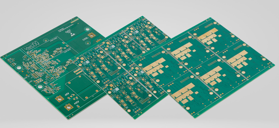
20+ Layer Backplane-Grade Satellite Communication PCB
A Satellite Communication PCB with more than 20 layers is a critical interconnection platform for high-capacity signal transmission and multi-module communication systems. Designed for demanding aerospace environments, this type of board combines high-density routing, controlled electrical performance, mechanical stability, and long-term reliability.
As satellite communication systems continue to increase data rates and integrate more functions into compact platforms, advanced High-Layer-Count PCB technology is becoming increasingly important for maintaining signal integrity and reliable system operation.
1. Advanced Material Selection for Demanding Environments
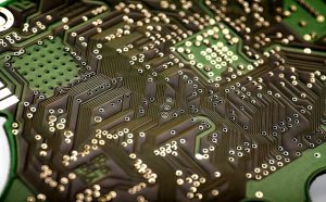
Satellite communication equipment operates under demanding environmental conditions, making material selection a critical part of Multilayer PCB manufacturing.
High-performance applications may require low-loss laminates, high-Tg materials, and substrates with excellent dimensional stability. Depending on signal frequency, electrical performance, thermal requirements, and mechanical construction, material systems can be selected to support high-speed and high-frequency signal transmission.
For complex satellite communication designs, material selection should consider:
- Low dielectric loss
- Stable dielectric properties
- High thermal resistance
- Low moisture absorption
- Excellent dimensional stability
- Reliable multilayer lamination performance
The combination of suitable laminate systems and carefully controlled manufacturing processes helps maintain consistent electrical characteristics across complex multilayer structures.
GOPCBA provides advanced PCB Manufacturing Services for high-layer-count, high-speed, high-frequency, HDI, and other demanding PCB applications.
2. Precision Manufacturing for High-Layer-Count Structures
Manufacturing a 20+ layer Backplane PCB requires precise control over layer registration, interlayer connections, drilling, plating, lamination, and final board dimensions.
High-layer-count boards have more complex internal structures than conventional multilayer PCBs. Small deviations during lamination, drilling, or registration can accumulate across multiple layers and affect electrical performance or mechanical assembly.
Key manufacturing processes include:
Precision Lamination
Multilayer lamination requires carefully controlled temperature, pressure, resin flow, and curing conditions. Stable lamination helps minimize delamination, voids, dimensional variation, and other defects that could compromise long-term reliability.
For hybrid material constructions, the lamination process must also account for differences in thermal expansion and material characteristics.
Precision Drilling and Interconnection
Through-holes, blind vias, buried vias, and other interconnection structures must maintain accurate positions and dimensions across the entire multilayer stack.
For high-density designs, advanced microvia and HDI technologies can further increase routing density and provide greater flexibility in complex circuit structures. GOPCBA’s PCB Capabilities cover HDI, microvias, blind and buried vias, controlled impedance, and high-layer-count PCB manufacturing.
Fine-Line Circuit Formation
High-speed satellite communication systems may require fine traces and tightly controlled spacing to support dense routing and high-frequency signal transmission.
Accurate circuit formation helps maintain impedance characteristics and minimize unwanted signal coupling, especially when multiple high-speed channels are routed through a dense backplane structure.
3. Strict Quality Control for Reliable Performance
A high-layer-count Satellite Communication PCB requires consistent electrical and mechanical performance throughout the manufacturing process.
Quality control should begin with incoming materials and continue through fabrication, inspection, electrical testing, and final shipment.
Important inspection and verification processes can include:
- Dimensional inspection
- Layer registration verification
- Copper thickness inspection
- Plating thickness inspection
- Impedance testing
- Electrical continuity and isolation testing
- Automated optical inspection
- X-ray inspection when required
- Final visual inspection
For high-speed and high-frequency applications, impedance control is particularly important. Variations in trace geometry, dielectric thickness, copper thickness, or material characteristics can affect signal transmission performance.
GOPCBA supports PCB Testing and Inspection as part of its integrated PCB and PCBA manufacturing capabilities, helping customers verify product quality before final delivery.
4. Engineering Support for Advanced Satellite PCBs
The successful production of a 20+ layer High-Layer-Count PCB depends not only on manufacturing equipment but also on engineering expertise.
Complex satellite communication boards require careful consideration of stack-up structure, material compatibility, impedance requirements, routing density, thermal management, and manufacturing feasibility.
An experienced PCB manufacturing partner can provide engineering support such as:
- Gerber file review
- DFM analysis
- Stack-up optimization
- Impedance evaluation
- Material selection
- Manufacturing feasibility analysis
- Lamination planning
- Drill and via optimization
Early engineering review can identify potential manufacturing risks before production, reducing unnecessary design revisions and improving production consistency.
For high-speed and RF-related designs, GOPCBA also provides High-Frequency PCB Manufacturing using specialized laminates and controlled-impedance manufacturing processes for demanding signal-transmission applications.
5. Why 20+ Layer Backplane PCBs Matter in Satellite Communication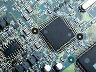
The primary value of a 20+ layer Backplane PCB is its ability to provide high routing density while maintaining organized power, ground, and signal structures.
A carefully engineered multilayer stack-up can provide:
High-Density Signal Routing
Multiple signal layers allow complex communication systems to accommodate a large number of high-speed channels without requiring an excessively large board footprint.
Improved Signal Integrity
Dedicated reference planes and controlled impedance structures can help reduce electromagnetic coupling, reflections, crosstalk, and signal loss.
Efficient Power and Ground Distribution
Dedicated power and ground layers provide more stable electrical distribution and help isolate sensitive high-speed signal paths from power-related interference.
Mechanical and Structural Stability
A high-layer-count backplane can provide the physical support required for multiple modules and connectors while maintaining dimensional stability during assembly and operation.
6. Applications of High-Layer Satellite Communication PCBs
20+ layer PCBs can be used in demanding satellite and aerospace electronics, including:
- Satellite communication systems
- RF communication equipment
- High-speed data processing systems
- Satellite networking platforms
- Aerospace computing equipment
- Communication backplanes
- Radar and microwave electronics
- High-density signal interconnection systems
As satellite systems evolve toward higher bandwidth, greater processing capacity, and more compact architectures, PCB technology must continue to advance accordingly.
7. GOPCBA High-Layer-Count PCB Manufacturing
GOPCBA provides advanced PCB fabrication and PCBA manufacturing for complex electronic applications, including high-layer-count, multilayer, HDI, high-frequency, high-speed, rigid-flex, heavy-copper, and controlled-impedance PCB technologies.
From prototype development to production manufacturing, GOPCBA supports engineering review, material selection, stack-up development, fabrication, inspection, and assembly.
For demanding satellite communication and aerospace electronics, a reliable Satellite Communication PCB requires more than a high layer count. Material selection, multilayer registration, impedance control, signal integrity, manufacturing precision, and quality verification must work together to achieve stable performance.
With advanced manufacturing capabilities and integrated engineering support, GOPCBA provides a practical manufacturing solution for complex High-Layer-Count PCB and Backplane PCB projects.