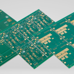
78-Layer Orthogonal Backplane PCB – Structure, Materials & Applications
With the rapid advancement of artificial intelligence (AI), high‑performance computing (HPC), cloud data centers, and next‑generation communication networks, the demand for high‑speed interconnect architectures has never been greater. Traditional backplanes often struggle with signal loss, crosstalk, and thermal constraints when supporting 112G PAM4, 224G PAM4, and beyond.
To address these challenges, many high‑end systems are adopting orthogonal backplane architectures. Among them, the 78‑layer orthogonal backplane PCB represents one of the most advanced technologies in high‑layer‑count PCB manufacturing. It is widely used in AI servers, core switches, cloud platforms, supercomputers, and telecom equipment. This article provides a complete analysis of its structural design, material selection, manufacturing processes, applications, and cost drivers.
1. What Is a 78‑Layer Orthogonal Backplane PCB?
A 78‑layer orthogonal backplane PCB is an ultra‑large multilayer board with up to 78 layers, designed for high‑speed interconnects within large electronic systems. Unlike traditional parallel backplanes, the orthogonal design arranges line cards and fabric cards at 90° angles, significantly shortening signal paths.
Key features include:
- Layer count up to 78 or higher
- Supports 112G PAM4 and 224G PAM4 signaling
- Extra‑large dimensions
- Ultra‑low‑loss materials
- High reliability and tight impedance control
Typical parameters: 60–80+ layers, thickness 10–18 mm, maximum size 800×600 mm, differential impedance 85Ω/100Ω, data rates up to 224G PAM4.
2. Orthogonal Backplane Architecture Explained
In a conventional backplane, all line cards plug in parallel, leading to long signal paths, high insertion loss, severe crosstalk, and obstructed airflow. The orthogonal backplane rotates the fabric cards 90°, offering:
- Shorter signal paths – reducing attenuation for high‑speed signals.
- Higher system bandwidth – meeting 400G/800G/1.6T Ethernet demands.
- Better thermal performance – smoother airflow paths improve cooling.
- Higher routing density – supporting more high‑speed channels.
3. Typical Layer Stack‑up of a 78‑Layer Orthogonal Backplane
A 78‑layer board uses a complex hybrid stack‑up:
- Signal layers (30–40 layers): high‑speed differential pairs, SerDes channels, and fabric switching.
- Ground layers (20–25 layers): provide return paths, EMI suppression, and signal integrity.
- Power layers (10–15 layers): deliver core voltages, high‑current distribution, and power integrity.
- Shielding layers: isolate high‑speed signals and reduce crosstalk.
The stack‑up is typically highly symmetrical to minimise warpage.
4. Material Selection for Ultra‑High‑Layer Backplanes
For 112G/224G systems, material choice directly determines signal quality.
- Panasonic Megtron 6: ultra‑low loss, excellent dimensional stability, high reliability – used in AI servers, HPC, and data center switches.
- Tachyon 100G: ultra‑low Df and insertion loss, ideal for core routers and telecom switches.
- Isola I‑Speed: balances performance and cost for enterprise networking and industrial communications.
Key material targets: Dk 3.0–3.5, Df ≤ 0.005, Tg ≥ 180°C.
5. Signal Integrity Design for 78‑Layer Backplanes
Signal integrity (SI) is critical. Key aspects include:
- Impedance control: 85Ω or 100Ω differential, typically ±5% tolerance.
- Insertion loss: target < 28 dB at Nyquist frequency.
- Crosstalk mitigation: increased spacing, ground planes, and orthogonal routing.
- Backdrill: almost mandatory to remove via stubs, reduce reflections, and improve eye diagrams.
- Connector matching: connectors must support 112G/224G PAM4 to ensure end‑to‑end channel performance.
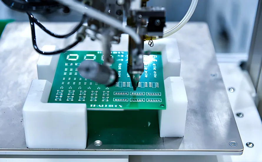
6. Manufacturing Challenges of 78‑Layer Orthogonal Backplanes
This is one of the most difficult PCB types to manufacture:
- Multiple laminations: typically 4–8 pressing cycles.
- Layer‑to‑layer registration: ≤ 50 μm alignment accuracy.
- Deep‑hole drilling: aspect ratios often exceed 15:1.
- Copper thickness uniformity: critical to avoid warpage, delamination, and stress imbalance.
- Extra‑large dimensions: many panels exceed 600 mm, requiring specialised large‑scale equipment.
7. IPC Standards and Reliability Requirements
High‑end backplanes are manufactured to IPC‑6012 Class 3 (high‑reliability), IPC‑A‑600 (acceptability), IPC‑2221 (design), and IPC‑4101 (materials).
8. Inspection and Testing
Typical tests include AOI, X‑ray, flying probe, metallographic cross‑section, thermal stress, and IST (interconnect stress testing).
9. Key Applications
- AI servers: GPU servers, training/inference clusters.
- Data centers: 800G switches, spine‑leaf architectures, cloud networking.
- Telecom: core routers, carrier switches, optical transport.
- Supercomputers: scientific computing, HPC clusters, national labs.
10. DFM Recommendations
- Maintain symmetrical stack‑up to reduce warpage.
- Optimise via structures with backdrill, via shielding, and stub‑free design.
- Balance copper distribution to avoid large copper areas.
- Confirm material availability early – ultra‑low‑loss materials have long lead times.
- Perform SI simulation for insertion/return loss, crosstalk, and eye margin.
For expert DFM support, visit our PCB design & layout service.
11. 2026 Price Reference for 78‑Layer Orthogonal Backplane PCBs
As one of the most advanced PCB products, pricing reflects high layer count, large size, expensive materials, and complex processes.
- Prototype (1–5 pcs): $8,000–20,000 per board
- Low volume (10–50 pcs): $5,000–12,000 per board
- Medium volume (50–200 pcs): $3,000–8,000 per board
Major cost drivers: layer count, material brand and loss grade, board thickness, number of backdrills, impedance requirements, testing scope, and IPC class.
12. Why Choose gopcb for 78‑Layer Orthogonal Backplane Manufacturing?
As a professional high‑end PCB manufacturer, gopcb provides advanced backplane solutions for global telecom, AI server, industrial control, and data center clients.
- Processing capabilities for Megtron, Tachyon, and Isola high‑speed materials
- High‑precision backdrill and large‑format board production
- Strict impedance control and IPC Class 3 compliance
- Full inspection: AOI, X‑ray, flying probe, cross‑section, thermal stress
- Free DFM review, stack‑up optimisation, and SI design support
Explore our PCB manufacturing and turnkey assembly services for complete system integration.
13. Frequently Asked Questions
Q1: What are the main applications of 78‑layer orthogonal backplanes?
AI servers, hyperscale data centers, telecom switches, core routers, aerospace, and supercomputers.
Q2: Why does orthogonal backplane outperform traditional designs?
Shorter signal paths reduce insertion loss and crosstalk, while improving thermal efficiency and system bandwidth.
Q3: Is backdrill mandatory for 78‑layer boards?
For 112G/224G systems, backdrill is standard to eliminate via stub reflections and ensure signal quality.
Q4: Which materials are best for 78‑layer high‑speed backplanes?
Panasonic Megtron 6, Tachyon 100G, and Isola I‑Speed are commonly used for their low loss and high reliability.
Q5: What is the typical lead time for a 78‑layer orthogonal backplane?
Prototypes: 6–10 weeks; volume production: 8–14 weeks, depending on material procurement and complexity.
14. Conclusion
As AI model training, 800G switching, and future 1.6T interconnects evolve, the 78‑layer orthogonal backplane PCB has become a fundamental enabler of next‑generation high‑performance systems. Its design, material selection, signal integrity, and manufacturing represent the highest level of PCB technology.
gopcb combines deep expertise in ultra‑high‑layer backplanes with advanced equipment and a rigorous quality system to help customers achieve reliable, high‑performance interconnects for the most demanding applications.
Get started with our prototype PCB assembly or high‑volume assembly services to bring your high‑speed designs to production.