High-speed PCB design does not end when the layout is completed. To achieve stable signal integrity, predictable impedance, and reliable performance at multi-gigabit data rates, the PCB must be manufactured using the right materials, a carefully engineered stack-up, and tightly controlled fabrication processes.
As interfaces such as PCIe, USB, Ethernet, DDR, HDMI, and high-speed networking continue to evolve, PCB traces, vias, connectors, and layer transitions increasingly behave as transmission-line structures. This means that PCB manufacturing quality can directly influence the electrical performance of the final system.
For this reason, successful high-speed PCB manufacturing requires close cooperation between the design team and the PCB manufacturer from the earliest stages of development.
This guide examines high-speed PCB fabrication from a manufacturer’s perspective, covering material selection, stack-up engineering, controlled impedance, drilling and plating, DFM review, inspection, and collaboration strategies. It also explains how Kingda supports high-speed PCB projects from engineering review and prototyping to PCB fabrication and PCBA assembly.
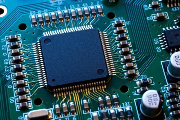
What Is a High-Speed PCB and Why Does Manufacturing Matter?
A high-speed PCB is a circuit board designed to carry fast digital, RF, or high-frequency signals where transmission-line effects can no longer be ignored.
There is no universal frequency threshold that defines a high-speed PCB. In practice, a board becomes increasingly sensitive to high-speed effects as signal rise time becomes shorter and the electrical length of the interconnect becomes significant.
Typical high-speed applications include:
- PCIe
- USB 3.x and newer interfaces
- High-speed Ethernet
- DDR memory
- SATA
- HDMI
- DisplayPort
- 5G communication
- AI computing
- High-performance servers
- Automotive radar and ADAS
- High-frequency RF systems
At these speeds, small variations in trace width, dielectric thickness, copper roughness, via geometry, and layer registration can affect impedance and signal quality.
A PCB may therefore pass a layout simulation but still experience unexpected signal-integrity problems if the manufacturing process does not reproduce the intended physical geometry accurately.
This is why high-speed PCB fabrication should be treated as an extension of the electrical design rather than a separate manufacturing activity.
High-Speed PCB Design vs. PCB Manufacturing: Who Does What?
A successful high-speed PCB project requires clearly defined responsibilities between the design team and the fabricator.
The design team is generally responsible for:
- Circuit architecture
- Schematic design
- Component selection
- PCB placement
- Signal routing
- Differential pairs
- Length matching
- Signal-integrity simulation
- Power-integrity analysis
- System-level validation
The manufacturer is responsible for converting the design into a physical board while maintaining the specified manufacturing parameters.
A capable high-speed PCB manufacturer should be able to:
- Review manufacturing data
- Evaluate stack-up feasibility
- Recommend practical materials
- Confirm impedance targets
- Review line width and spacing
- Validate via structures
- Control lamination
- Control etching
- Control copper plating
- Monitor layer-to-layer registration
- Perform impedance testing
- Verify finished-board quality
The manufacturer should not replace the engineering design process, but should provide practical feedback about whether the proposed design can be built consistently at production scale.
This distinction is important because DFM for high-speed PCBs is not the same as redesigning the circuit. The manufacturer evaluates manufacturability and process capability, while the designer remains responsible for signal behavior and system architecture.
Materials for High-Speed PCB Manufacturing
Material selection is one of the most important variables affecting high-speed PCB performance.
Standard FR-4 materials can support many moderate-speed applications. However, as data rates increase or signal paths become longer, dielectric loss and material variation become increasingly important.
Key material parameters include:
- Dielectric constant (Dk)
- Dissipation factor (Df)
- Copper roughness
- Glass-weave structure
- Moisture absorption
- Thermal stability
- Coefficient of thermal expansion
- Mechanical strength
Enhanced FR-4 and High-Speed Laminates
Enhanced FR-4 materials can provide improved electrical performance compared with conventional FR-4 while maintaining relatively good cost efficiency and manufacturability.
These materials are often suitable for:
- High-speed digital interfaces
- Networking equipment
- Industrial controllers
- Computing hardware
- Automotive electronics
Low-Loss Laminates
For more demanding high-speed channels, low-loss laminates can reduce signal attenuation and improve channel performance.
Examples of material families used in advanced high-speed designs include hydrocarbon-based laminates and other low-loss dielectric systems.
PTFE and Ultra-Low-Loss Materials
For RF, microwave, and millimeter-wave applications, PTFE-based or other ultra-low-loss materials may be required.
These materials provide excellent high-frequency performance but typically introduce additional manufacturing complexity and cost.
The best material is therefore not necessarily the one with the lowest Df. It must also be:
Electrically suitable + mechanically stable + manufacturable + available + economically practical.
Kingda can support customers in selecting PCB materials according to project requirements, including electrical performance, thermal conditions, mechanical requirements, and intended production volume.
High-Speed PCB Stack-Up and Controlled Impedance
The PCB stack-up is the foundation of controlled-impedance design.
It defines the relationship between signal layers, reference planes, dielectric thickness, and copper geometry.
A high-speed stack-up should provide:
- Stable reference planes
- Controlled dielectric thickness
- Consistent copper thickness
- Appropriate signal-to-plane spacing
- Balanced construction
- Reliable impedance characteristics
For example, the characteristic impedance of a microstrip or stripline depends heavily on:
- Trace width
- Copper thickness
- Dielectric thickness
- Dielectric constant
- Reference-plane distance
- Conductor geometry
Therefore, a generic impedance calculator is only an initial design tool. The final stack-up should be confirmed against the materials and fabrication process that will actually be used.
Why Stack-Up Collaboration Matters
One of the most common mistakes in high-speed PCB design is finalizing the layout using a theoretical stack-up and only later discovering that the fabricator cannot reproduce it reliably.
A better process is:
Manufacturer consultation → Stack-up proposal → Impedance calculation → Layout → DFM review → Fabrication → Coupon testing → Validation
This approach reduces the gap between simulation and actual hardware.
Controlled Impedance Manufacturing
For a controlled-impedance PCB, manufacturing consistency is critical.
The manufacturer must control:
- Trace width
- Trace thickness
- Dielectric thickness
- Copper plating
- Etching rate
- Layer registration
- Lamination conditions
- Material properties
Even relatively small dimensional variations can affect impedance.
For this reason, professional high-speed PCB manufacturers commonly use test coupons manufactured alongside production boards.
These coupons allow impedance measurements to be taken using Time Domain Reflectometry (TDR) or equivalent techniques.
The resulting data can be compared against:
- Target impedance
- Measured impedance
- Simulation models
- Design tolerances
This provides a direct connection between the theoretical design and the manufactured PCB.
Key Manufacturing Capabilities for Reliable High-Speed PCBs
Not every multilayer PCB manufacturer is qualified to produce demanding high-speed boards.
Important capabilities include the following.
Trace Width and Etching Control
Trace geometry strongly affects impedance.
A capable manufacturer should be able to maintain consistent etching across:
- Large panels
- Fine-line inner layers
- Fine-line outer layers
- High-density routing areas
Consistent etching helps reduce impedance variation from board to board and panel to panel.
Advanced Via and Drilling Technology
Vias can introduce discontinuities into high-speed signal paths.
Depending on the design, manufacturers may need to support:
- Through-hole vias
- Blind vias
- Buried vias
- Microvias
- Stacked microvias
- Via-in-pad
- Copper-filled vias
- Back-drilling
For high-speed interfaces, shorter via stubs can reduce unwanted resonances and reflections.
The manufacturer must therefore control:
- Drill diameter
- Drill depth
- Registration
- Hole-wall quality
- Plating thickness
- Aspect ratio
Copper Plating Quality
Copper plating affects both electrical and mechanical reliability.
Uniform plating ensures:
- Stable via resistance
- Reliable interlayer connections
- Consistent copper thickness
- Better thermal cycling performance
For demanding high-speed applications, cross-section analysis can be used to verify plating quality and layer structure.
Layer-to-Layer Registration
Registration accuracy is especially important for high-density and high-speed multilayer PCBs.
Misalignment can alter:
- Trace-to-plane spacing
- Via-to-pad alignment
- Annular ring dimensions
- Differential-pair geometry
- Impedance characteristics
Manufacturers therefore need accurate registration systems and stable lamination processes.
Surface Finish Selection for High-Speed PCBs
Surface finish primarily affects solderability and corrosion protection, but conductor surface characteristics can also influence high-frequency performance.
Common finishes include:
- ENIG
- ENEPIG
- Immersion Silver
- Immersion Tin
- OSP
- Hard Gold
The appropriate finish depends on:
- Component package
- Assembly method
- Reliability requirements
- Shelf life
- Environmental conditions
- Signal-frequency requirements
For fine-pitch SMT and BGA assemblies, flat surface finishes such as ENIG are widely used because of their good solderability and dimensional consistency.
For extremely high-frequency applications, designers should also evaluate conductor roughness and the electrical impact of the selected surface construction.
High-Speed PCB DFM Review
A DFM review for high-speed PCB manufacturing should go beyond basic trace-and-spacing checks.
A capable manufacturer should evaluate whether the proposed board can be manufactured within the physical tolerances necessary to achieve the required electrical performance.
What Should a High-Speed DFM Review Cover?
Stack-Up Feasibility
The manufacturer should confirm:
- Layer count
- Core availability
- Prepreg availability
- Copper weights
- Press-cycle compatibility
- Final dielectric thickness
Impedance Feasibility
The manufacturer should verify whether the requested impedance values can realistically be achieved with the proposed stack-up and trace geometries.
Trace Width and Spacing
Minimum design dimensions must remain within the manufacturer’s stable production window.
This is especially important for:
- Fine-line inner layers
- Differential pairs
- RF traces
- HDI structures
Via Structure Review
The manufacturer should verify:
- Drill size
- Aspect ratio
- Via type
- Via filling requirements
- Back-drilling requirements
- Registration limits
Material Compatibility
The selected laminate and prepreg system should be compatible with the required:
- Layer count
- Lamination cycle
- Copper thickness
- Surface finish
- Thermal requirements
Reference Plane Continuity
Large openings, slots, anti-pads, and plane splits near high-speed routing should be reviewed because they may create return-path discontinuities.
What High-Speed DFM Does Not Cover
It is important to understand the boundaries of manufacturer-led DFM.
A PCB fabricator generally does not replace the hardware design team in:
- Signal-integrity simulation
- Timing analysis
- Circuit topology
- Component selection
- Termination design
- Differential-pair strategy
- System-level validation
The manufacturer’s role is to ensure that the submitted physical design can be manufactured reliably and consistently.
Good cooperation therefore requires both sides to understand their responsibilities.
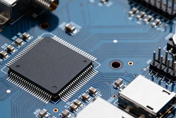
How to Work Effectively with a High-Speed PCB Manufacturer
Engage the Manufacturer Before Layout Is Finalized
One of the most effective ways to reduce design iterations is to involve the fabricator early.
Before routing is locked, the manufacturer can help confirm:
- Material availability
- Recommended stack-up
- Dielectric thickness
- Copper weights
- Impedance targets
- Minimum line/space
- Via capabilities
- Production constraints
This prevents designers from developing a layout around a stack-up that later proves impractical.
Provide Complete Manufacturing Documentation
A high-speed PCB manufacturing package should ideally include:
- Gerber files
- ODB++ or IPC-2581 data where applicable
- NC drill files
- Complete stack-up drawing
- Material specifications
- Copper weights
- Finished board thickness
- Impedance table
- Controlled-impedance routing information
- Via specifications
- Surface finish requirements
- Special-process requirements
A clear and complete manufacturing package reduces misunderstandings and speeds up DFM review.
Confirm Impedance Coupon Testing
For controlled-impedance boards, ask your manufacturer whether the production panel includes impedance test coupons.
The test report should ideally identify:
- Test structure
- Target impedance
- Measured impedance
- Tolerance
- Test method
- Production lot
This data provides objective evidence that the manufactured board matches the intended electrical design.
Plan Prototype and Mass Production Together
A prototype material may not always be the best choice for mass production.
Some advanced laminates may be:
- Expensive
- Difficult to source
- Subject to long lead times
- Less scalable
- More complicated to process
A manufacturer that understands your future production roadmap can recommend materials and stack-ups that minimize the risk of requalification later.
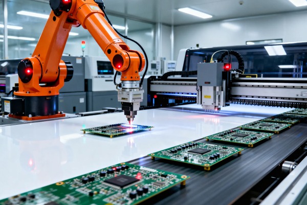
High-Speed PCB Manufacturing Process
A typical high-speed PCB manufacturing workflow includes:
Design Data Review → DFM & CAM Engineering → Stack-Up Confirmation → Inner-Layer Imaging → Etching & AOI → Layer Stack-Up → Lamination → Mechanical/Laser Drilling → Desmear & Electroless Copper → Outer-Layer Imaging → Copper Plating → Etching → Solder Mask → Silkscreen → Surface Finish → Electrical Testing → Impedance Testing → Final Inspection → Depanelization → Packaging & Shipment
This process shows why high-speed PCB manufacturing is a system of tightly controlled operations rather than simply a faster version of conventional PCB fabrication.
High-Speed PCB Manufacturing Capabilities
For reference, high-speed PCB manufacturing programs may require capabilities such as:
| Capability | Typical Advanced Requirement |
|---|---|
| Layer Count | 2–40 layers |
| Minimum Trace / Space | Down to approximately 2.5 / 2.5 mil, depending on board construction |
| Minimum Mechanical Drill | Approximately 0.15 mm |
| Laser Microvia | Approximately 0.10 mm or smaller, depending on process |
| Controlled Impedance | Typically targeted within ±5% where specified |
| Board Size | Project-dependent |
| Finished Thickness | Project-dependent |
| Copper Weight | Application-dependent |
| Through-Hole Aspect Ratio | Application-dependent |
| Impedance Testing | TDR coupon testing where required |
These values should always be confirmed against the manufacturer’s current process capability before layout is finalized.
High-Speed PCB Materials
Depending on electrical performance requirements, high-speed PCB projects may use:
Enhanced FR-4
Suitable for many high-speed digital interfaces where cost and manufacturing efficiency remain important.
Mid-Loss and Low-Loss Laminates
Suitable for more demanding multi-gigabit systems and mixed-signal applications.
PTFE-Based Materials
Used for RF and microwave designs requiring extremely low dielectric loss.
Hybrid Stack-Ups
Combining different materials can help balance:
Performance + Cost + Manufacturability
Hybrid construction can be particularly useful when only certain signal layers require premium low-loss materials.
Special Processes for High-Speed PCBs
Advanced high-speed designs may require:
- Blind and buried vias
- Laser microvias
- Via-in-pad
- Resin-filled and copper-capped vias
- Back-drilling
- HDI build-up
- Sequential lamination
- TDR impedance testing
- Cross-section analysis
Each special process increases manufacturing complexity, so early engineering review is essential.
Why Choose Kingda for High-Speed PCB Manufacturing?
Kingda can provide an integrated PCB manufacturing and PCBA assembly workflow, helping hardware teams manage high-speed PCB projects from prototype through production.
One-Stop PCB and PCBA Manufacturing
Instead of coordinating multiple vendors for fabrication, component sourcing, and assembly, Kingda can integrate:
- PCB fabrication
- Component procurement
- SMT assembly
- Through-hole assembly
- AOI inspection
- X-ray inspection
- Electrical testing
- Functional testing
- Box-build integration
This integrated model simplifies project communication and improves manufacturing continuity.
Engineering and DFM Support
Kingda’s engineering support can help customers review:
- Gerber files
- BOM
- Pick-and-place data
- Stack-up
- DFM
- DFA
- Component availability
- Manufacturing risks
Early engineering involvement helps identify production risks before fabrication begins.
Support From Prototype to Production
High-speed hardware usually requires multiple engineering iterations.
Kingda can support the transition from:
Prototype → Engineering Validation → Low-Volume Production → Mass Production
Using the same manufacturing partner can reduce the risk of process inconsistencies during production transfer.
Advanced PCB Technology Support
Kingda supports demanding PCB requirements including:
- Multilayer PCB
- HDI PCB
- Rigid PCB
- Flexible PCB
- Rigid-flex PCB
- High-density PCB
- Fine-pitch PCB
- High-frequency and high-speed PCB applications
Specific material and process availability should be confirmed during project review.
Integrated Component Sourcing
High-speed boards often contain specialized processors, memory devices, connectors, power-management components, and other long-lead components.
Kingda can support BOM analysis, component sourcing, lifecycle review, alternative recommendations, and procurement coordination, helping reduce supply-chain risks during prototype and production stages.
Quality and Inspection
High-speed PCB quality depends not only on the bare board but also on assembly quality.
Kingda can integrate inspection technologies such as:
- SPI
- AOI
- X-ray
- ICT
- Functional testing
This provides greater visibility across the complete PCBA manufacturing process.
Checklist for Selecting a High-Speed PCB Manufacturer
Before selecting a supplier, ask the following questions:
Materials
- Does the manufacturer support low-loss PCB laminates?
- Are the preferred materials regularly stocked?
- Can alternative materials be proposed without compromising performance?
Stack-Up
- Can the manufacturer provide a practical production stack-up?
- Can dielectric thickness be controlled after lamination?
- Can the manufacturer support the required impedance?
Fabrication
- What are the minimum line/space capabilities?
- What via structures are supported?
- Is back-drilling available?
- Can the manufacturer provide HDI and microvia structures?
Quality
- Is impedance coupon testing available?
- Are TDR reports provided?
- Is cross-section analysis available?
- How is layer registration controlled?
Assembly
- Can the factory handle fine-pitch BGA and QFN packages?
- Is X-ray inspection available?
- Can ICT and functional testing be performed?
Production
- Can the same supplier support prototype and mass production?
- Can component sourcing be handled internally?
- Is full production traceability available?
These questions help distinguish a general PCB supplier from a manufacturer with genuine high-speed PCB manufacturing capabilities.
Conclusion
Successful high-speed PCB manufacturing requires much more than simply producing a multilayer board.
As data rates continue to increase, the final PCB must accurately reproduce the electrical assumptions established during design. Stack-up architecture, material selection, controlled impedance, trace geometry, copper roughness, via structures, layer registration, plating quality, and testing all contribute to the final signal-integrity performance.
The most effective approach is to involve the PCB manufacturer before the layout is fully locked. By collaborating on the stack-up, material selection, impedance targets, DFM requirements, and manufacturing tolerances, engineers can reduce the gap between simulation and real hardware.
For companies developing AI hardware, high-speed networking, telecom equipment, automotive electronics, data-center systems, medical devices, and other advanced electronic products, a capable high-speed PCB manufacturer can become an important engineering partner rather than simply a supplier.
With integrated PCB fabrication, component sourcing, PCB assembly, inspection, DFM engineering, and production support, Kingda provides a practical one-stop manufacturing path for high-speed PCB projects from prototype through production.