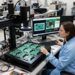
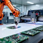
As electronic devices become faster, more compact, and increasingly data-intensive, maintaining signal integrity, controlling impedance, and managing thermal performance have become essential challenges in modern electronics.
At the center of these requirements are high-speed PCBs, which provide the electrical infrastructure needed to transmit large volumes of data rapidly and reliably. From artificial intelligence servers and 5G communication equipment to automotive electronics, medical devices, and high-performance computing systems, high-speed PCB technology plays a critical role in enabling next-generation electronic products.
Unlike conventional circuit boards, high-speed PCBs require much more careful consideration of transmission-line effects, signal integrity, power integrity, electromagnetic compatibility, material selection, and manufacturing tolerances.
This guide provides a comprehensive overview of high-speed PCB design, manufacturing considerations, applications, common challenges, and future development trends, while explaining how Kingda supports customers from PCB design and fabrication to assembly and testing.
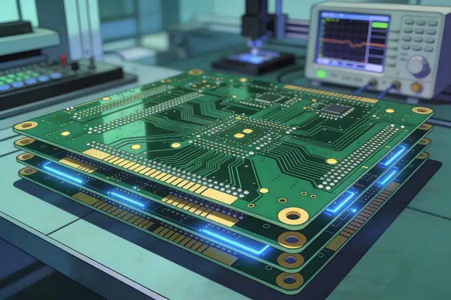
What Are High-Speed PCBs?
A high-speed PCB is a printed circuit board designed to transmit signals at sufficiently high edge rates or frequencies where transmission-line effects can no longer be ignored.
There is no single universal frequency threshold that defines a high-speed PCB. In practice, whether a board should be treated as “high speed” depends not only on clock frequency but also on signal rise time, trace length, interconnect geometry, impedance, and the electrical behavior of the system.
When signal transitions become fast enough, PCB traces behave like transmission lines. Effects such as reflections, crosstalk, insertion loss, return loss, propagation delay, and impedance discontinuities can significantly affect system performance.
High-speed PCBs are therefore commonly used in applications such as:
- High-performance computing
- AI servers and accelerators
- Data storage systems
- Telecommunications
- 5G infrastructure
- Automotive electronics
- ADAS and autonomous driving
- Industrial networking
- Medical imaging
- Consumer electronics
The goal of a high-speed PCB is not simply to transmit signals quickly. It must transmit them cleanly, consistently, and with minimal distortion.
High-Speed PCB vs. Standard PCB
The fundamental difference between a high-speed PCB and a conventional PCB lies in how electrical signals behave on the board and how carefully those effects must be controlled.
| Feature | High-Speed PCB | Standard PCB |
|---|---|---|
| Signal Edge Rate | Fast transitions require transmission-line analysis | Slower transitions are generally less sensitive |
| Signal Integrity | Critical design consideration | Often less demanding |
| Impedance Control | Precise controlled impedance is commonly required | Usually less stringent |
| Crosstalk | Must be carefully controlled | Often less critical |
| Return Path | Continuous return paths are essential | Simpler grounding may be sufficient |
| Stackup | Carefully engineered dielectric structure | More conventional layer configuration |
| Materials | May require low-loss/high-frequency laminates | Standard FR-4 often sufficient |
| Design Complexity | High | Moderate to low |
| Manufacturing Tolerance | Tighter | Generally more relaxed |
| Cost | Typically higher | Generally lower |
For conventional circuits operating at relatively low edge rates, simple trace routing may be sufficient. However, as data rates increase, a trace is no longer merely a copper connection. It becomes part of the signal transmission system.
That is why high-speed PCB design requires both electrical engineering knowledge and manufacturing expertise.
Key Challenges in High-Speed PCB Design
Designing a reliable high-speed printed circuit board involves several interconnected engineering challenges.
1. Signal Integrity
Signal integrity is one of the most important considerations in high-speed PCB design.
A high-speed signal can be distorted by:
- Reflections
- Crosstalk
- Overshoot and undershoot
- Insertion loss
- Impedance discontinuities
- Via transitions
- Connector discontinuities
- Excessive trace length
Poor signal integrity can produce data errors, timing problems, intermittent failures, or unstable system behavior.
Engineers should therefore use signal-integrity simulation and carefully control trace geometry, dielectric thickness, reference planes, and routing topology.
2. Controlled Impedance
Impedance control is fundamental to high-speed PCB performance.
The characteristic impedance of a transmission line depends on several factors, including:
- Trace width
- Trace thickness
- Dielectric thickness
- Dielectric constant
- Copper roughness
- Reference-plane configuration
Common controlled-impedance targets include 50 Ω single-ended and 90 Ω or 100 Ω differential, although the actual requirement depends on the interface and system architecture.
For example, high-speed differential interfaces may require tightly matched differential impedance and controlled pair geometry.
Manufacturers should validate impedance through stackup calculations, field-solver modeling, and, where required, test coupons and laboratory measurements.
3. Return Path Management
A high-speed signal requires a complete current loop.
When a signal changes layers, crosses reference planes, or encounters gaps in a ground structure, the return current can be forced to take a longer path.
This may result in:
- Increased EMI
- Higher inductance
- Signal distortion
- Greater crosstalk
- Impedance discontinuities
For this reason, designers should provide continuous reference planes and use appropriately positioned ground vias when changing signal layers.
Good return-path design is particularly important for multi-layer high-speed PCBs.
4. Crosstalk and Electromagnetic Interference
When two high-speed traces run closely together, electromagnetic coupling can cause unwanted interference.
This is known as crosstalk.
Crosstalk can be reduced by:
- Increasing spacing between sensitive traces
- Minimizing long parallel routing
- Using continuous reference planes
- Separating noisy and sensitive circuits
- Controlling layer orientation
- Optimizing trace geometry
The classic “3W” spacing guideline can be useful as an initial layout rule, but it should not replace actual signal-integrity analysis.
Proper EMI/EMC design is also essential for products requiring regulatory certification and reliable operation in electrically noisy environments.
5. Thermal Management
Although high-speed PCB design is primarily associated with signal integrity, thermal management should not be overlooked.
Modern processors, networking ICs, power-management devices, AI accelerators, and high-speed transceivers can generate substantial heat.
Excessive temperature can affect:
- Component reliability
- Signal performance
- Timing stability
- Solder-joint life
- System lifetime
Thermal design may involve:
- Copper planes
- Thermal vias
- Heat sinks
- Metal-core structures
- Thermal interface materials
- Advanced PCB laminates
- Optimized component placement
Electrical and thermal design should therefore be considered together rather than treated as separate engineering tasks.
Power Integrity in High-Speed PCB Design
Power integrity (PI) is closely related to signal integrity.
Modern high-speed ICs can switch large currents within very short time intervals. If the power-distribution network cannot provide stable voltage, the resulting noise may affect system performance.
Engineers should consider:
- Power-plane design
- Ground-plane continuity
- Decoupling capacitor placement
- Capacitor selection
- PDN impedance
- Via inductance
- Current density
Decoupling capacitors should be placed as close as practical to the relevant power pins, while low-inductance connections should be used to minimize transient voltage fluctuations.
For complex high-speed products, SI/PI co-simulation can help identify problems before fabrication.
High-Speed PCB Design Considerations
A successful high-speed design begins long before routing.
Layer Stackup
The PCB stackup forms the foundation of high-speed performance.
Engineers should carefully define:
- Number of signal layers
- Power and ground layers
- Dielectric thickness
- Copper thickness
- Material dielectric constant
- Loss tangent
- Symmetry
- Impedance targets
A well-designed stackup improves signal integrity and simplifies impedance control.
Material Selection
Standard FR-4 can work well for many moderate-speed applications, but higher-performance interfaces may require low-loss PCB materials.
Material selection should consider:
- Dielectric constant (Dk)
- Dissipation factor (Df)
- Thermal stability
- Moisture resistance
- Copper roughness
- Coefficient of thermal expansion
- Mechanical reliability
For high-frequency or long-channel applications, low-loss materials can reduce signal attenuation and improve overall link performance.
Differential Pair Routing
Many high-speed interfaces rely on differential signaling.
Examples include:
- PCIe
- USB
- Ethernet
- Display interfaces
- High-speed memory
- Serial communication interfaces
Differential pairs should be routed with:
- Controlled spacing
- Consistent impedance
- Length matching where required
- Minimal unnecessary vias
- Consistent reference planes
- Smooth layer transitions
High-Speed PCB Manufacturing Considerations
Design quality alone does not guarantee high-speed performance.
The manufacturing process must reproduce the design accurately enough to maintain the electrical characteristics established during simulation.
1. Stackup Control
Manufacturers must maintain consistent dielectric thickness and material properties.
Even small variations in dielectric geometry can affect controlled impedance.
2. Trace Geometry Control
Trace width and copper thickness influence impedance.
Therefore, high-speed PCB manufacturing requires tighter process control over:
- Line width
- Line spacing
- Copper thickness
- Etching variation
- Registration
3. Drilling and Via Quality
Poor via geometry can introduce unwanted inductance and impedance discontinuities.
High-speed boards may require:
- Laser-drilled microvias
- Blind vias
- Buried vias
- Back drilling
- Via-in-pad
- Copper-filled vias
The correct structure depends on the electrical and packaging requirements of the board.
4. Copper Plating
Reliable copper plating is necessary for both electrical performance and mechanical durability.
Important parameters include:
- Hole-wall copper thickness
- Surface copper thickness
- Plating uniformity
- Adhesion
- Aspect ratio capability
5. Surface Finish
Common finishes include:
- ENIG
- ENEPIG
- HASL
- OSP
- Immersion Silver
For fine-pitch and high-density applications, flat surface finishes such as ENIG are often preferred for assembly consistency.
High-Speed PCB Assembly
After fabrication, high-speed PCB assembly introduces another set of engineering requirements.
Component Placement
High-speed components should be placed according to signal-flow priorities.
For example:
- Processors and memory should be positioned close together where required.
- High-speed connectors should be located to minimize routing length.
- Clock sources should be isolated from noisy power circuits.
- Sensitive analog circuits should be separated from high-noise digital switching areas.
SMT Assembly
Modern high-speed boards often use fine-pitch components, including:
- BGA
- QFP
- QFN
- LGA
- CSP
- 0201 and smaller passive components
Precise solder paste printing and component placement are therefore essential.
Reflow Soldering
An optimized reflow profile helps ensure reliable solder joints without exceeding component thermal limits.
Inspection
High-speed assemblies may require:
- SPI
- AOI
- X-ray
- ICT
- Functional testing
X-ray inspection is particularly useful for BGA packages with hidden solder joints.
Applications of High-Speed PCBs
The demand for high-speed printed circuit boards continues to expand across multiple industries.
Telecommunications
Telecommunications infrastructure relies on high-speed circuitry for:
- Routers
- Network switches
- Optical communication
- Base stations
- Data transport equipment
- 5G infrastructure
Reliable high-speed interconnects are essential for moving large quantities of data with low latency.
Aerospace and Defense
Aerospace electronics require high-speed signal processing for:
- Radar
- Navigation
- Communication
- Avionics
- Electronic warfare systems
These boards must maintain reliable electrical performance while operating under demanding environmental conditions.
Automotive Electronics
Modern vehicles contain increasingly complex electronic architectures.
High-speed automotive PCBs are used in:
- ADAS
- Autonomous driving
- Vehicle networking
- Radar
- Infotainment
- Smart cockpit systems
- Battery management
- Domain controllers
AI and High-Performance Computing
AI servers and HPC systems represent some of the most demanding high-speed PCB applications.
These systems require:
- High-speed processors
- High-bandwidth memory
- High-speed networking
- High-density power delivery
- Advanced thermal management
PCB designs must support both high data throughput and extremely stable power delivery.
Consumer Electronics
Smartphones, laptops, tablets, routers, wearables, and gaming systems increasingly depend on high-speed interconnects.
Compact form factors make HDI and advanced multilayer technologies particularly valuable.
Medical Electronics
High-speed PCBs are used in:
- CT scanners
- MRI systems
- Ultrasound equipment
- Patient monitoring systems
- Medical imaging
- Laboratory equipment
Signal accuracy and reliability are particularly important when the PCB processes sensitive medical data.
Industrial Electronics
Industrial applications include:
- Machine vision
- Industrial Ethernet
- Robotics
- Automated inspection
- Control systems
- Data acquisition
These products often require reliable high-speed communications in electrically noisy environments.
Future Trends in High-Speed PCB Technology
The future of high-speed PCB technology will be shaped by several major trends.
Advanced Low-Loss Materials
As data rates increase, conventional materials may not provide sufficient electrical performance.
The industry is increasingly adopting materials with:
- Lower dielectric loss
- More stable Dk
- Lower surface roughness
- Better thermal performance
Advanced materials will become increasingly important for high-frequency networking, AI computing, 5G/6G infrastructure, and high-speed optical-electrical systems.
AI-Assisted PCB Design
Artificial intelligence is increasingly being applied to PCB design workflows.
Potential applications include:
- Automated placement optimization
- Routing assistance
- Signal-integrity analysis
- Thermal optimization
- Constraint checking
- DFM analysis
AI-assisted engineering will allow designers to evaluate more design alternatives in less time.
Greater HDI Integration
As products become smaller while data rates rise, HDI PCB technology will become increasingly important.
Microvias, sequential lamination, fine-line routing, and advanced packaging technologies can increase routing density while reducing board size.
5G and Future Wireless Networks
High-frequency communication systems require PCBs capable of supporting increasingly demanding RF and digital interfaces.
Future wireless systems will create further demand for:
- Low-loss laminates
- RF/microwave PCB materials
- Precise impedance control
- Integrated antenna structures
- Advanced electromagnetic simulation
Advanced Thermal Management
Increasing processor density means that future PCBs will need better thermal solutions.
Possible approaches include:
- Embedded copper
- Metal-core structures
- Advanced heat spreaders
- Integrated thermal vias
- High-conductivity materials
How Kingda Supports High-Speed PCB Projects
Selecting the right high-speed PCB manufacturer is just as important as selecting the correct materials and design tools.
Kingda provides an integrated PCB manufacturing and PCBA assembly solution designed to support customers from prototype through production.
Professional Engineering Support
Kingda can support customers with:
- DFM analysis
- DFA review
- Stackup planning
- Impedance-control recommendations
- Gerber review
- Component sourcing
- Manufacturing optimization
- Prototype development
Early engineering review helps identify potential manufacturability and signal-integrity issues before production begins.
High-Speed PCB Manufacturing
Kingda supports advanced PCB technologies for demanding applications, including:
- Multilayer PCBs
- HDI PCBs
- High-frequency PCBs
- Rigid PCBs
- Flexible PCBs
- Rigid-flex PCBs
Material selection can be optimized according to electrical, thermal, mechanical, and environmental requirements.
High-Precision PCB Assembly
For high-speed PCB assembly, Kingda provides SMT and through-hole assembly capabilities for fine-pitch and high-density components.
Inspection and testing can include:
- SPI
- AOI
- X-ray
- ICT
- Functional testing
This creates a closed manufacturing loop from PCB fabrication through assembled-board validation.
One-Stop Manufacturing
Instead of coordinating multiple suppliers for PCB fabrication, component procurement, assembly, and testing, customers can work with Kingda through a more integrated manufacturing workflow.
This helps:
- Reduce communication gaps
- Improve project coordination
- Shorten procurement cycles
- Improve engineering consistency
- Simplify quality management
- Support prototype-to-production scaling
Quality and Reliability Focus
For high-speed applications, consistency matters as much as nominal capability.
Kingda emphasizes process control, engineering review, inspection, and manufacturing traceability to help customers achieve reliable and repeatable PCB performance.
Frequently Asked Questions About High-Speed PCBs
What Is the Difference Between a High-Speed PCB and a Normal PCB?
A high-speed PCB is designed for signals where transmission-line effects significantly influence system performance. It generally requires tighter control of impedance, routing, return paths, crosstalk, and signal integrity than a conventional PCB.
What Data Rates Can High-Speed PCBs Support?
There is no universal data-rate limit for the category. Modern high-speed PCB designs can support interfaces ranging from several gigabits per second to much higher data rates, depending on the material, stackup, channel length, component technology, and manufacturing quality.
What Materials Are Used for High-Speed PCBs?
Standard FR-4 can support many high-speed applications, while more demanding RF and high-data-rate designs may use low-loss laminates with controlled dielectric properties and lower dissipation factors.
Why Is Impedance Control Important?
Controlled impedance helps reduce signal reflections and maintain predictable transmission-line behavior. It is especially important for differential and high-frequency interfaces.
How Can High-Speed PCB Signal Integrity Be Improved?
Key practices include:
Controlled impedance + continuous return paths + proper layer stackup + short routing + reduced vias + differential-pair control + crosstalk management + SI/PI simulation
Conclusion
High-speed PCB technology has become a critical foundation for modern electronics as data rates, processing power, and system complexity continue to increase.
A successful high-speed PCB design requires more than simply increasing the number of layers. Engineers must carefully consider:
- Signal integrity
- Power integrity
- Controlled impedance
- Return paths
- Crosstalk
- EMI/EMC
- Thermal management
- Material selection
- Manufacturing tolerances
- Assembly quality
As AI, 5G, high-performance computing, automotive electronics, and advanced medical systems continue to develop, demand for reliable high-speed printed circuit boards will continue to grow.
The key to success is collaboration between the PCB designer, engineering team, and manufacturing partner from the earliest design stage. With the right stackup, materials, simulation strategy, fabrication process, and assembly controls, high-speed PCB technology can deliver the signal integrity, reliability, and performance required by next-generation electronics.
Kingda combines high-speed PCB manufacturing, advanced multilayer and HDI capabilities, PCB assembly, component sourcing, DFM engineering, inspection, and testing to support electronics companies from prototype development to production.