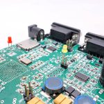
In modern electronics manufacturing, consistent PCB Quality Inspection is essential for ensuring electrical performance, dimensional accuracy, assembly compatibility, and long-term product reliability. As PCB structures become increasingly complex, manufacturers must apply systematic inspection criteria to substrates, copper conductors, plated holes, solder masks, surface finishes, silkscreens, board dimensions, and mechanical characteristics.
For Double-Sided PCBs and Multilayer PCBs, quality requirements can vary according to the product application, material system, manufacturing process, and customer specifications. Internationally recognized IPC Standards provide important guidelines for PCB quality evaluation, while the final acceptance criteria should always be based on the applicable product specification and the agreement between the PCB manufacturer and customer.
Kingda applies a comprehensive PCB Quality Control approach throughout the manufacturing process, helping customers identify potential defects and maintain stable production quality.
The following inspection guidelines summarize key areas that should be considered when evaluating finished PCBs.
1. Scope of PCB Quality Inspection
This inspection standard covers the primary quality characteristics of finished printed circuit boards, including:
- Base material and substrate condition
- Copper conductors
- Plated and non-plated holes
- Pads and lands
- Solder mask
- Surface finish and tin plating
- Gold fingers
- Silkscreen and text markings
- Board dimensions and profile
- Warpage and twist
- Solderability
- Thermal resistance
- General appearance and workmanship
If a particular requirement is not covered by the applicable IPC Standards, or if the customer’s specification differs from the general inspection criteria, the customer-approved specification should take precedence.
2. Base Material and Substrate Inspection
The substrate is the structural foundation of a PCB. Defects in the laminate can affect mechanical strength, electrical insulation, thermal performance, and long-term PCB Reliability.
2.1 White Spots and Woven Glass Fiber Exposure
White spots or areas of visible glass-fiber texture may be acceptable when they remain within the limits defined by the applicable specification.
As a general reference:
- The affected area should not exceed approximately 5% of the total board area.
- White spots occurring within line spacing should not occupy more than 50% of the available spacing.
Acceptance limits should ultimately be determined according to the board material, product class, and customer requirements.
2.2 Delamination and Blistering
Delamination, blistering, separation between material layers, or lifting of copper foil should not be present.
The substrate should maintain sufficient adhesion between copper foil, dielectric material, and internal layers throughout the expected operating conditions.
2.3 Foreign Material
Foreign matter on the substrate may be acceptable only when it satisfies the applicable inspection limits. As a general reference, the foreign material should:
- Be identifiable as a non-conductive substance.
- Reduce the original conductor spacing by no more than 50%.
- Have a maximum dimension of approximately 0.75 mm.
Foreign conductive particles that could create a short circuit are not acceptable.
2.4 Fiber and Copper Foil Condition
The base material should not show exposed internal fibers, severe delamination, or lifting of copper foil. Any material defect that may reduce dielectric strength or mechanical integrity should be rejected.
2.5 Material Specification
The laminate type, thickness, dielectric characteristics, and other material properties should conform to the approved drawing, material specification, or customer requirements.
3. PCB Thickness and Warpage Tolerance
Board thickness is an important dimensional characteristic for both Double-Sided PCBs and Multilayer PCBs.
The finished board thickness should meet the customer-approved specification, taking into account copper thickness, dielectric construction, surface finish, and manufacturing tolerances.
Typical reference tolerances for rigid PCB thickness may include:
| Board Thickness | Double-Sided PCB | Multilayer PCB |
|---|---|---|
| 0.2–1.0 mm | ±0.10 mm | — |
| 1.2–1.6 mm | ±0.13 mm | ±0.15 mm |
| 2.0–2.6 mm | ±0.18 mm | ±0.18 mm |
| Above 3.0 mm | ±0.18 mm | ±0.20 mm |
These values should be treated as reference values rather than universal limits. The applicable drawing and manufacturing specification should be used for final acceptance.
Warpage and twist should also remain within the specified limits because excessive deformation may cause problems during SMT, through-hole assembly, connector installation, or enclosure integration.

4. Hole Inspection Requirements
Hole quality is critical to electrical interconnection and mechanical assembly.
Both plated through holes (PTH) and non-plated through holes (NPTH) should be inspected for diameter, position, shape, cleanliness, plating condition, and internal defects.
4.1 Hole Diameter Tolerance
Typical reference tolerances may include:
| Finished Hole Diameter | PTH Tolerance | NPTH Tolerance |
|---|---|---|
| Less than 1.6 mm | ±0.08 mm | ±0.05 mm |
| Greater than 1.6 mm | ±0.10 mm | ±0.05 mm |
The actual tolerance should follow the customer drawing and the manufacturer’s current process capability.
Hole location should also comply with the approved PCB fabrication data.
4.2 Missing and Blocked Holes
The following defects should not be present:
- Missing holes
- Unfinished holes
- Incorrectly drilled holes
- Blocked holes
- Unintended closed holes
4.3 Hole Shape
Deformed holes are not acceptable when they affect component insertion, electrical connectivity, or dimensional requirements.
Examples include:
- Circular holes drilled into an oval shape
- Oval holes drilled into a circular shape
- Excessive bell-mouth or trumpet-shaped holes
- Other abnormal drilling deformation
4.4 Hole Contamination
Copper residues, solder residues, debris, or other contaminants inside holes should not reduce the final hole diameter or interfere with component insertion and electrical connection.
4.5 Internal Hole Wall Defects
Localized exposed copper or defects on the inner hole wall should remain within the applicable inspection limits.
For plated holes, the copper plating should provide continuous electrical and mechanical connection between the relevant layers.
4.6 Voids and Cavities
Voids in plated hole walls should be controlled according to the applicable quality class and customer requirements. Excessive void area, multiple voids, continuous annular voids, or damage that compromises hole-wall integrity should not be accepted.
Plated through holes connecting internal layers should maintain reliable electrical continuity.
4.7 Non-Conductive Through Holes
Unintended non-conductive defects in plated through holes are not acceptable when they compromise the required electrical connection.
4.8 Plating Condition Inside Holes
The plating inside holes should:
- Maintain the required plating thickness.
- Provide reliable electrical continuity.
- Have good adhesion to the hole wall.
- Be free from severe wrinkles, cracks, peeling, or separation.
5. Pad and Land Inspection
Pads provide the physical interface between PCB conductors and electronic components. Their dimensions, shape, and integrity directly influence solderability and assembly reliability.
The annular ring around a drilled hole should remain sufficient after drilling and registration tolerances are considered.
As a general reference, the remaining annular ring should maintain an adequate connection width and should not be excessively reduced by hole offset.
Small pinholes or surface defects may be acceptable within the limits defined by the applicable product specification, provided that they do not compromise solderability or electrical performance.
For SMD pads, surface imperfections should not significantly reduce the effective soldering area.
Pads should also be free from:
- Severe copper reduction
- Excessive scratches
- Peeling
- Contamination
- Unintended solder mask coverage
6. Conductor and Trace Inspection
Conductors are among the most important items in PCB Quality Inspection.
Short circuits and open circuits are not acceptable.
Minor conductor imperfections may be acceptable only when they remain within the limits of the applicable specification and do not compromise electrical performance.
Typical inspection considerations include:
- Trace width
- Trace spacing
- Copper thickness
- Conductor continuity
- Edge roughness
- Pinholes
- Nicks
- Scratches
- Voids
- Local protrusions or recesses
As a general reference, conductor width and spacing should remain within the agreed manufacturing tolerance.
For example, a trace-width deviation of approximately ±20% may be used as a reference in certain specifications, but this should not replace the customer’s actual drawing or applicable IPC Standards.
The following conditions should generally be rejected:
- Short circuits
- Open circuits
- Severe conductor deformation
- Excessive saw-tooth edges
- Conductor breaks
- Copper loss that compromises the required electrical width
For high-density Multilayer PCBs, conductor inspection becomes increasingly important because fine-line structures have smaller process margins.
7. Solder Mask Inspection
The solder mask protects copper conductors and helps prevent unintended solder bridging during assembly.
The solder mask type, color, ink system, and manufacturer should comply with the approved customer specification.
The solder mask should be:
- Uniformly applied
- Properly cured
- Well adhered
- Free from significant bubbling
- Free from peeling
- Free from excessive contamination
As a process reference, solder mask thickness should be controlled according to the manufacturer’s material and process specifications rather than applying one fixed thickness to every PCB.
7.1 Solder Mask Adhesion
A tape adhesion test may be performed according to the approved inspection procedure. After the specified tape is applied and removed, the solder mask should not exhibit unacceptable peeling or lifting.
7.2 Solder Mask Repair
Localized solder mask repair may be acceptable when permitted by the applicable specification. Repaired areas should be smooth, firmly bonded, and visually consistent with the surrounding surface.
7.3 Solder Mask Contamination
Foreign fibers and other non-conductive contaminants should not bridge conductors or interfere with soldering.
Components holes intended for assembly should remain free of unintended solder mask unless the design specifically requires plugged or tented holes.
8. Surface Finish and Plating Inspection
Surface finish affects solderability, corrosion resistance, contact performance, and long-term PCB Reliability.
The plated surface should be uniform and free from severe roughness, peeling, blistering, fingerprints, oxidation, contamination, and discoloration.
8.1 Plating Adhesion
A suitable tape adhesion test may be performed according to the approved inspection procedure. Plating should not peel or blister under normal testing conditions.
8.2 Plating Thickness
Copper, nickel, gold, tin, or other surface finishes should meet the thickness requirements specified in the customer’s drawing or manufacturing specification.
For example, the applicable specification may define minimum copper or nickel thickness for plated holes and contact areas.
Thickness should be measured using an appropriate inspection method rather than relying solely on visual inspection.
8.3 Tin-Sprayed Surface
For tin-sprayed boards, the surface should be smooth and uniform, with no severe contamination, discoloration, or defects that could affect solderability.
The coating should not excessively reduce hole diameter.
8.4 Electroless Nickel/Gold or Other Gold Finishes
For gold-finished PCBs, the copper, nickel, and gold layers should meet the specified thickness requirements.
The gold surface should have a consistent appearance and should be free from:
- Oxidation
- Contamination
- Discoloration
- Peeling
- Severe scratches
- Exposed underlying metal where not permitted
9. PCB Surface and Appearance Inspection
The overall PCB surface should be clean and free from defects that could affect function, assembly, or appearance.
The following conditions should be carefully inspected:
- Scratches
- Exposed substrate
- Copper residues
- Ink contamination
- Oil stains
- Adhesive residue
- Fingerprints
- Corrosion residue
- Foreign material
Scratches that expose the substrate or underlying metal should be evaluated according to the applicable product specification.
Minor cosmetic marks may be acceptable only when they do not affect electrical performance, solderability, mechanical integrity, or customer appearance requirements.
10. Gold Finger Inspection
Gold fingers are commonly used for edge connectors and require strict dimensional and surface-quality control.
The nickel and gold layers should meet the specified thickness requirements.
Gold fingers should be:
- Uniform in appearance
- Free from oxidation
- Free from severe contamination
- Free from burning or discoloration
- Free from peeling
- Free from excessive scratches
- Free from exposed copper or nickel where not permitted
The edges of gold fingers should not be lifted, cracked, or seriously damaged.
Small scratches or localized surface imperfections may be accepted only when they remain within the agreed specification and do not affect electrical contact reliability.
A tape adhesion test may also be used to verify the bonding strength of the surface finish.
The contact area should remain sufficiently clean and intact to ensure reliable insertion and electrical connection.
11. Silkscreen and Text Marking Inspection
Silkscreen provides important information for PCB assembly, inspection, maintenance, and troubleshooting.
Text and symbols should comply with the customer’s requirements for:
- Position
- Color
- Ink type
- Content
- Orientation
- Layer
- Legibility
Characters should be clear, complete, and easy to identify.
Unless specifically permitted by the design, silkscreen should not overlap:
- Solder pads
- SMD land patterns
- Component leads
- Through-hole openings
Polarity symbols, pin-1 indicators, component reference designators, and other assembly markings must be accurate.
Unclear or incomplete characters that could cause misidentification should not be accepted.
Tape adhesion testing may be used where required to verify that printed characters remain firmly attached to the PCB surface.
12. Marking and Identification
When required by the customer, the PCB may include specific identification marks such as:
- Manufacturer logo
- Customer logo
- UL marking
- Manufacturing date
- Customer part number
- Material identification
- Flammability marking
- Revision information
The correct marking layer and location should be verified during PCB Quality Inspection.
All identification marks should be complete, legible, and consistent with the approved manufacturing documentation.
13. Board Dimensions and Mechanical Processing
Dimensional accuracy is particularly important when PCBs must be installed into connectors, housings, mechanical assemblies, or automated production equipment.
Typical reference tolerances may include:
| Manufacturing Method | Dimensional Tolerance |
|---|---|
| CNC Milling | ±0.15–0.20 mm |
| Punching | Approximately ±0.15 mm |
Actual tolerances should be determined by the customer drawing and the manufacturer’s process capability.
For irregular holes and slots, dimensional accuracy and the distance between the feature center and board edge should also be controlled.
Milled edges and slots should be smooth and free from excessive burrs, copper exposure, cracking, or mechanical damage.
For punched boards, the edges should be clean and free from unacceptable breakout.
14. V-Cut and Depanelization Quality
For PCBs manufactured with V-cut scoring, the remaining board thickness should be uniform and consistent with the approved specification.
As a reference:
| Board Thickness | Typical Remaining Thickness |
|---|---|
| 0.8–1.0 mm | 0.2–0.3 mm |
| 1.2 mm | 0.3–0.4 mm |
| 1.6 mm | 0.4–0.5 mm |
| 2.0 mm | 0.5–0.6 mm |
| 2.5 mm | 0.5–0.7 mm |
For boards thinner than approximately 0.8 mm, V-cut requirements should be agreed separately.
The V-cut line should be straight and uniform and should not damage copper conductors.
15. Solderability Inspection
Solderability is a critical part of PCB Quality Control because surface oxidation and contamination can directly affect assembly yield.
A typical solderability evaluation may use a solder temperature around 245 ± 5°C, a suitable flux system, and a controlled immersion time according to the applicable standard.
The soldered area should wet properly and should not show unacceptable dewetting or non-wetting.
After solderability testing:
- Solder mask should remain firmly attached.
- Silkscreen should not blister or peel.
- Hole barrels should not exhibit unacceptable separation.
- The substrate should remain free from delamination.
- Board warpage should remain within the specified limits.
The exact test parameters should follow the applicable IPC Standards, customer requirements, and product class.
16. Thermal Shock and Thermal Stress Testing
Thermal shock testing evaluates the ability of a PCB to withstand rapid temperature changes and soldering-related thermal stress.
A typical test may involve multiple solder immersions at approximately 288°C for a specified duration, depending on the applicable standard and qualification procedure.
After testing, the following defects should not occur:
- Substrate delamination
- Copper foil lifting
- Blistering
- Internal-layer separation
- Plated-hole cracking
- Plating delamination
- Blow holes or excessive voiding
For Multilayer PCBs, thermal stress testing is particularly important because repeated heating can reveal weaknesses in interlayer bonding and plated-through-hole structures.
17. Kingda’s Approach to PCB Quality Control
Consistent quality requires more than final visual inspection. Effective PCB Quality Control should begin with material verification and continue through imaging, drilling, plating, etching, solder mask application, surface finishing, electrical testing, and final inspection.
At Kingda, inspection can be integrated into the manufacturing process to help identify potential defects before they become downstream assembly problems.
Key inspection areas include:
- Incoming material verification
- Layer registration
- Trace width and spacing
- Drilling accuracy
- Hole-wall quality
- Copper and plating thickness
- Solder mask condition
- Surface finish
- Gold finger quality
- Board dimensions
- Electrical continuity
- Solderability
- Final visual inspection
For complex Multilayer PCBs, process control and inspection data are especially important because small manufacturing deviations can affect multiple layers simultaneously.
18. Conclusion
A comprehensive PCB Quality Inspection system is essential for maintaining consistent performance and reliability in modern electronics.
For Double-Sided PCBs and Multilayer PCBs, inspection should cover not only appearance but also dimensional accuracy, conductor integrity, plated-hole quality, solder mask, surface finish, mechanical properties, solderability, and thermal resistance.
Although IPC Standards provide an important foundation for PCB quality evaluation, the final acceptance criteria should always consider the product class, design requirements, manufacturing process, and customer specifications.
By combining process control, inspection technology, manufacturing expertise, and DFM-oriented engineering, Kingda can help customers achieve stable production quality and improve overall PCB Reliability.
As PCB structures continue to become finer, denser, and more complex, systematic PCB Quality Control will remain a key factor in achieving reliable and consistent electronic products.