Multilayer PCB Manufacturing Process: A Complete Step-by-Step Guide
Multilayer PCB manufacturing is a precise and systematic process in which every production stage directly affects the electrical performance, mechanical strength, reliability, and service life of the finished circuit board. From raw material preparation and inner-layer fabrication to lamination, drilling, outer-layer processing, surface finishing, testing, and final packaging, the complete process involves numerous critical operations and quality control checkpoints.
For manufacturers and electronic product developers, understanding the Multilayer PCB Manufacturing process is important for evaluating production feasibility, improving product reliability, and reducing manufacturing risks. A well-controlled production process ensures that the finished multilayer PCB meets the required electrical, dimensional, and reliability specifications.
1. Inner Layer Fabrication: Building the Foundation of a Multilayer PCB
The inner layer is one of the most important foundations of a multilayer circuit board. Its circuit patterns must be accurately transferred and processed before the individual layers can be combined into a complete multilayer structure.
Material Cutting
Production begins with cutting the original PCB laminate according to the dimensions specified in the engineering documentation. Proper material preparation provides the correct starting dimensions for subsequent processing.
The selection and preparation of PCB materials should also correspond to the electrical, thermal, mechanical, and application requirements of the final product.
Dry Film Lamination
After the material is prepared, a photosensitive dry film is laminated onto the copper surface of the inner-layer material. This dry film serves as the imaging medium for transferring the required circuit pattern.
Inner Layer Exposure
During exposure, specialized imaging equipment transfers the designed circuit pattern onto the dry film. The exposed photosensitive areas undergo a chemical change, creating the pattern required for subsequent development.
Inner Layer Developing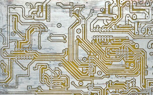
The developing process removes the unexposed dry film and exposes the copper areas that need to be etched. Accurate developing is essential because any deviation can affect the final conductor pattern.
Inner Layer Etching
The exposed copper is removed through a controlled chemical etching process, leaving the designed inner-layer circuitry on the PCB material.
The accuracy of this stage directly affects conductor width, spacing, and overall circuit integrity.
Inner-Layer AOI Inspection
Automated Optical Inspection (AOI) is performed after etching to identify potential defects such as:
- Open circuits
- Short circuits
- Abnormal trace widths
- Pattern defects
- Other visual abnormalities
Early inspection helps prevent defective inner layers from proceeding to later production stages.
Brown Oxide Treatment
Brown oxide treatment creates an oxide layer on the surface of the inner-layer copper. This treatment improves the bonding strength between the inner copper layers and the prepreg during lamination and helps reduce the risk of delamination.
2. Lamination and Pre-Outer-Layer Processing
After the inner layers are completed and inspected, they must be accurately aligned and combined to form the multilayer PCB structure.
Multilayer Lamination
Lamination combines the inner circuit layers with prepreg materials under controlled temperature and pressure.
This process creates the integrated multilayer PCB structure. Precise control of temperature, pressure, alignment, and lamination parameters is essential for maintaining dimensional stability and interlayer reliability.
For projects requiring complete board production rather than PCB assembly alone, PCB Fabrication capabilities are particularly important because multilayer structures depend heavily on accurate layer registration and controlled manufacturing processes.
Board Edge Routing
After lamination, the board edges are trimmed and routed to achieve the required dimensions and remove excess material.
Drilling
Drilling creates the holes required for electrical and mechanical connections between PCB layers. Depending on the design, multilayer boards may contain through-holes, blind vias, and other specialized hole structures.
Blind-via designs may require additional processing steps compared with standard through-hole structures.
Plasma Treatment
After drilling, plasma treatment can be used to clean and condition the hole walls. It helps remove contaminants and drilling residues while improving the surface condition of the hole walls for subsequent copper deposition.
Deburring
Deburring removes burrs and residues generated during mechanical processing. Maintaining a clean and smooth board surface helps improve the consistency of subsequent manufacturing operations.
Electroless Copper Plating
A thin layer of copper is chemically deposited onto the hole walls and board surfaces. This conductive layer provides the foundation for subsequent electroplating and establishes the electrical connection between PCB layers.
Panel Plating
The copper layer is then electroplated to increase its thickness to the required specification. Proper copper thickness is important for electrical connectivity, current-carrying capability, and long-term reliability.
For complex electronic products, integrating PCB fabrication with assembly capabilities can also simplify the overall supply chain. GOPCBA provides both manufacturing and assembly solutions for projects ranging from prototypes to production volumes.
3. Outer Layer Fabrication: Creating the External Circuitry
The outer-layer manufacturing process creates the external conductive patterns and prepares the PCB surface for soldering and component assembly.
Outer Layer Dry Film, Exposure, and Developing
The outer-layer circuit pattern is transferred to the PCB surface through processes similar to those used for inner-layer fabrication.
Dry film is applied, the required pattern is exposed, and the unexposed film is developed to reveal the areas requiring further processing.
Dry Film Inspection
The developed dry film is inspected to confirm that the transferred circuit pattern is accurate and free from obvious defects.
Pattern Plating
Selective electroplating increases the copper thickness of the external circuit areas. The required copper thickness depends on the electrical and mechanical requirements of the PCB design.
Outer Layer Etching
The copper that is not protected by the plated pattern is removed through controlled etching, leaving the final external circuit pattern.
Outer-Layer AOI Inspection
AOI is performed to inspect the finished outer-layer circuitry and identify potential open circuits, shorts, trace defects, and other pattern abnormalities.
Consistent inspection is a key element of PCB Quality Control, particularly for high-density and multilayer PCB designs where manufacturing defects can affect multiple electrical connections.
4. Solder Mask Processing
After the external circuitry has been completed and inspected, the PCB surface is prepared for solder mask application.
Surface Preparation
The PCB surface is cleaned and conditioned to remove oxidation, contamination, and other residues. Proper surface preparation improves the adhesion and consistency of the solder mask.
Solder Mask Application
A solder mask layer is applied to the PCB surface. Its primary purpose is to protect copper areas that do not need to be soldered and to reduce the risk of oxidation and unintended electrical shorts.
Pre-Baking, Exposure, and Developing
The solder mask is processed through pre-baking, exposure, and developing steps to create the required solder mask pattern.
The process exposes the pads and other areas that need to remain available for soldering.
Solder Mask Inspection
The finished solder mask is inspected to ensure that the pattern is accurate and free from defects such as missing coverage, excessive coverage, or other printing abnormalities.
5. Surface Finishing and Final PCB Processing
Surface finishing is an important stage in Multilayer PCB Manufacturing because the selected finish affects solderability, oxidation resistance, surface performance, and the suitability of the PCB for different applications.
Silkscreen Printing
Identification marks, component references, symbols, and other required information are printed onto the PCB surface. These markings can help during assembly, inspection, troubleshooting, and maintenance.
Curing
The solder mask and silkscreen are cured through controlled heating to stabilize their physical and functional properties.
Surface Finishing
Depending on the PCB design and application requirements, several surface finishing technologies may be used, including:
- ENIG
- HASL
- Lead-free HASL
- Immersion tin
- Immersion silver
- OSP
- Gold fingers
- ENEPIG
- Electroplated gold
Different surface finishes offer different combinations of solderability, oxidation resistance, durability, cost, and application suitability. Therefore, surface finishing should be selected according to the PCB’s intended operating environment and assembly requirements.
6. Electrical Testing and Final Inspection
After fabrication is completed, the finished PCB undergoes electrical and quality inspections before shipment.
Electrical Testing
Electrical testing verifies whether the PCB meets the required electrical specifications. Typical tests include:
- Continuity testing
- Insulation testing
- Electrical connection verification
These tests help identify electrical defects before the boards enter the assembly stage.
Final Routing and Profiling
The PCB is processed to achieve its final mechanical dimensions. Depending on the design, methods such as routing and V-scoring may be used.
Accurate profiling ensures that the PCB can be properly installed into the customer’s final product or assembly fixture.
Final Inspection
A comprehensive final inspection is performed to verify the appearance, dimensions, electrical characteristics, and overall quality of the finished circuit board.
A systematic PCB Manufacturing Process should maintain quality control throughout production rather than relying only on final inspection. Controlling critical parameters at each stage helps reduce defects and improve manufacturing consistency.
7. Packaging and Shipment
After passing all required inspections and tests, qualified multilayer PCBs are properly packaged for shipment.
Appropriate packaging helps protect the boards from moisture, contamination, mechanical damage, and environmental exposure during transportation and storage.
For projects that require both bare PCB fabrication and subsequent component assembly, an integrated manufacturing solution can further simplify procurement and production coordination. GOPCBA supports PCB fabrication together with component sourcing and PCB assembly services, allowing customers to manage multiple stages of electronic manufacturing through one supply chain.
Why Process Control Matters in Multilayer PCB Manufacturing
The multilayer PCB production process contains many interconnected manufacturing stages. A problem introduced during an early process may not become visible until a later stage, making process control especially important.
Several factors have a direct impact on final PCB quality:
Material Quality
PCB laminates, copper foil, prepreg, and other materials form the physical foundation of the circuit board. Material selection should match the electrical, thermal, mechanical, and reliability requirements of the application.
Layer Alignment
Accurate layer registration is essential for multilayer PCBs. Misalignment between layers can affect vias, pads, traces, and electrical connections.
Copper Thickness Control
Consistent copper thickness is important for current-carrying capability, electrical performance, and connection reliability.
Hole Quality
Drilling accuracy and hole-wall quality directly affect interlayer connections. Poor hole quality can result in unreliable electrical connections or manufacturing defects.
Surface Protection
Solder mask and surface finishing protect the PCB and prepare the board for component assembly. Selecting and controlling the appropriate surface finish helps maintain solderability and long-term reliability.
Inspection and Testing
AOI, electrical testing, dimensional inspection, and final quality checks provide important opportunities to detect defects before the PCB reaches the customer.
From Prototype to Production: Choosing the Right PCB Manufacturing Solution
Different electronic products require different production strategies. Prototype projects may prioritize fast engineering verification and design iteration, while low-volume and high-volume production require greater emphasis on process consistency, supply-chain coordination, production efficiency, and cost control.
For prototype development, Prototype PCB Assembly can help engineers validate PCB designs and assembly performance before moving into larger production quantities.
For projects requiring smaller production runs, Low Volume PCB Assembly provides a flexible option for products that are transitioning from prototype validation toward regular production.
When demand increases, High Volume PCB Assembly is designed to support larger production requirements with automated manufacturing processes and supply-chain coordination.
For customers seeking a complete electronics manufacturing solution, Turnkey PCB Assembly can integrate PCB fabrication, component procurement, assembly, inspection, testing, and related manufacturing services.
Conclusion
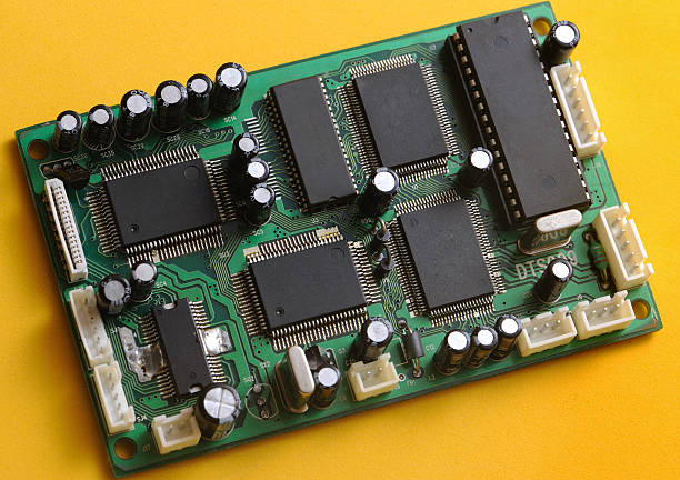
The complete Multilayer PCB Manufacturing process is a highly coordinated sequence that includes material preparation, inner-layer fabrication, AOI inspection, lamination, drilling, copper plating, outer-layer processing, solder mask application, surface finishing, electrical testing, final inspection, and packaging.
Every stage contributes to the final performance and reliability of the circuit board. Effective manufacturing therefore requires more than simply producing circuit patterns; it requires strict process control, accurate equipment, qualified materials, engineering support, and systematic inspection throughout the production cycle.
For electronic manufacturers, hardware developers, and engineering teams, understanding the complete PCB Manufacturing Process makes it easier to evaluate manufacturing risks, select appropriate production methods, and build reliable electronic products from prototype development through volume production.