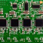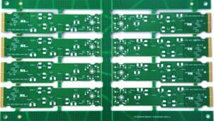
As the electronics industry continues to develop rapidly, circuit layouts are becoming increasingly dense and complex. This trend has created higher requirements for PCB manufacturing, particularly for high-density rigid-flex and flexible circuit applications.
During the PCB pattern transfer process, many manufacturers use dry film resist to protect selected copper areas during etching or electroplating. Compared with traditional liquid photoresist processes, dry film offers good process consistency and is well suited to fine-line circuit fabrication.
However, improper handling of dry film can result in defects such as pinholes, film cracking, poor adhesion, and electroplating leakage. These problems can negatively affect circuit definition, yield, and the reliability of the finished PCB.
This article explains the common causes of dry film defects and provides practical solutions that manufacturers such as Kingda can apply during PCB manufacturing.
1. Why Do Pinholes Appear in Dry Film?
One common defect is the appearance of pinholes or breaks in the dry film after lamination, exposure, or development.
Some operators assume that increasing the lamination temperature and pressure will improve adhesion and eliminate pinholes. In practice, excessive temperature or pressure can have the opposite effect.
The photosensitive resist layer contains solvents and other volatile components. If the temperature is too high, excessive solvent evaporation can cause the film to become thinner, drier, and more brittle. A brittle film is more susceptible to damage during development and subsequent processing.
The objective of dry film lamination is therefore not simply to maximize temperature and pressure. Instead, the process should achieve sufficient softening and intimate contact between the dry film and copper surface while maintaining the mechanical integrity of the resist layer.
Common Causes of Dry Film Pinholes
Several factors can contribute to pinholes or local film damage:
- Excessive lamination temperature
- Excessive lamination pressure
- Insufficient surface preparation
- Rough or contaminated copper surfaces
- Poor drilling or punching quality
- Insufficient exposure energy
- Excessive development pressure
- Excessive waiting time after lamination
- Excessive tension applied to the dry film during lamination
How to Reduce Dry Film Pinholes
The following measures can help improve the stability of the process:
1. Optimize lamination temperature and pressure
Do not automatically increase temperature and pressure when defects occur. The correct parameters should be established according to the dry film manufacturer’s specifications, copper surface condition, board thickness, and equipment characteristics.
2. Improve drilling and punching quality
Mechanical damage generated during drilling, routing, punching, or other processes can create local defects that subsequently develop into pinholes.
Drilling tools should be properly maintained, and burrs, debris, and contamination should be controlled.
3. Optimize exposure energy
Exposure must be sufficient to polymerize the photosensitive resist properly. Insufficient exposure can produce a weak resist pattern that is easily damaged during development.
4. Reduce excessive development pressure
Development pressure that is too high can mechanically attack weak or poorly polymerized resist areas. The pressure and spray conditions should therefore be optimized according to the dry film specifications and circuit pattern.
5. Control the dwell time after lamination
After dry film lamination, the panel should not be left for an unnecessarily long period before exposure. Excessive waiting can allow stress relaxation or changes in the partially softened resist layer, particularly around corners and uneven structures.
6. Avoid excessive film tension
The dry film should be laminated with controlled tension. Pulling the film excessively tight can cause uneven thickness or mechanical stress, which may contribute to defects during subsequent processing.
2. What Causes Electroplating Leakage Through Dry Film?
Another important defect is electroplating leakage, sometimes referred to as plating breakthrough.
This occurs when the dry film resist does not adequately protect the copper surface during electroplating. Plating solution can reach areas that should remain protected, causing unwanted copper deposition and potentially changing the designed circuit geometry.
Electroplating leakage is often associated with poor adhesion between the dry film and copper surface, incomplete polymerization, excessive film stress, or inappropriate lamination and exposure parameters.
Three major process variables are particularly important:
- Exposure energy
- Dry film temperature
- Lamination pressure
3. Exposure Energy and Dry Film Performance
Exposure energy is one of the most important parameters in the PCB pattern transfer process.
When exposed to ultraviolet light, the photoinitiators in the resist absorb energy and generate reactive species that initiate polymerization. The exposed resist becomes sufficiently cross-linked to resist the developer.
If the exposure energy is too low, polymerization may be incomplete. The resist can swell or soften during development, resulting in:
- Poor line definition
- Resist lifting
- Pattern distortion
- Reduced adhesion
- Local film removal
- Increased risk of electroplating leakage
On the other hand, excessive exposure can also create problems. Overexposure may make development more difficult and can cause unwanted resist residues or dimensional changes in the developed pattern.
Therefore, exposure energy should be controlled within an appropriate process window rather than simply being increased to improve adhesion.
For production lines, exposure calibration should be performed regularly because lamp aging, equipment conditions, dry film characteristics, and substrate surface conditions can affect the actual exposure dose.
4. The Effect of Dry Film Temperature
Temperature plays an important role during dry film lamination.
If the lamination temperature is too low, the resist may not soften sufficiently. As a result, the film may not flow properly into microscopic surface irregularities on the copper, reducing the contact area and weakening adhesion.
If the temperature is too high, however, solvents and volatile components within the resist may evaporate excessively. This can cause:
- Film drying
- Reduced flexibility
- Increased brittleness
- Bubble formation
- Uneven film thickness
- Poor adhesion
- Film lifting during electroplating
Therefore, the optimum temperature should provide adequate film flow without causing excessive solvent loss.
The actual setting should be determined according to the dry film specification, lamination equipment, copper surface condition, and board construction.
5. The Effect of Lamination Pressure
Lamination pressure must also be carefully controlled.
If the pressure is too low, the dry film may not make sufficient contact with the copper surface. Small gaps or uneven areas may remain between the resist and substrate, creating potential paths for plating solution.
This can result in:
- Poor adhesion
- Localized lifting
- Voids
- Electroplating leakage
- Pattern defects
However, excessive pressure is not necessarily beneficial.
Too much pressure can cause excessive deformation of the resist layer and may promote excessive displacement or thinning of the film. Combined with excessive temperature, it can also increase solvent loss and make the resist more brittle.
Therefore, the goal of lamination is to achieve uniform contact and stable adhesion—not simply maximum pressure.
6. Copper Surface Preparation Is Critical
The quality of the copper surface directly affects dry film adhesion.
Before lamination, the copper surface should be sufficiently clean and appropriately conditioned. Contamination from oil, dust, fingerprints, oxidation, or processing residues can reduce adhesion between the resist and copper.
Typical surface preparation may involve:
- Cleaning
- Micro-etching
- Surface roughening
- Water rinsing
- Drying
- Contamination control
The surface should provide enough micro-roughness to promote adhesion without being excessively rough.
For fine-line PCB manufacturing, surface preparation becomes even more important because small defects can have a significant impact on line definition and electrical performance.
7. Control the Entire Dry Film Process, Not Just One Parameter
Dry film defects are rarely caused by a single parameter.
For example, increasing exposure energy may not solve a problem caused by poor copper cleaning. Similarly, increasing lamination pressure cannot compensate for an improperly prepared copper surface.
A stable dry film process requires coordinated control of:
- Copper surface preparation
- Dry film storage
- Material handling
- Lamination temperature
- Lamination pressure
- Lamination speed
- Exposure energy
- Exposure uniformity
- Development pressure
- Development time
- Rinsing
- Drying
- Panel handling
The interaction between these parameters should be evaluated as a complete process window.
8. Proper Dry Film Storage and Handling
The quality of the dry film can also be affected before it reaches the lamination machine.
Dry film materials should be stored according to the supplier’s specified temperature, humidity, and shelf-life requirements.
Improper storage can change the physical and photosensitive properties of the material.
During handling, operators should also avoid:
- Touching the active surface directly
- Excessive bending
- Scratching
- Contamination
- Excessive stretching
- Prolonged exposure to unsuitable environmental conditions
Proper material handling is a simple but important part of maintaining consistent PCB quality.
9. Special Considerations for Rigid-Flex PCB Manufacturing
The requirements become more challenging when manufacturing a rigid-flex PCB.
Rigid-flex structures may contain different materials, thickness transitions, flexible areas, stiffeners, and complex three-dimensional structures. These features can make uniform dry film lamination more difficult than on a simple rigid board.
Potential challenges include:
- Uneven surface topography
- Thickness variation
- Material transition areas
- Flexible sections
- Stiffener edges
- Local stress concentration
- Fine-line circuit requirements
For this reason, manufacturers need to carefully evaluate the lamination process according to the actual rigid-flex construction.
In flexible areas, excessive mechanical stress should be avoided because the flexible substrate and copper circuitry can be more sensitive to bending and handling damage.
10. How to Troubleshoot Dry Film Breakthrough and Leakage
When a dry film defect occurs, a systematic troubleshooting approach is more effective than simply changing one process parameter.
A useful troubleshooting sequence includes:
Step 1: Inspect the copper surface
Check for contamination, oxidation, excessive roughness, or insufficient surface treatment.
Step 2: Check dry film storage conditions
Confirm that the material is within its shelf life and has been stored according to specifications.
Step 3: Verify lamination parameters
Review temperature, pressure, speed, and film tension.
Step 4: Verify exposure energy
Use exposure calibration or process monitoring to confirm that the actual exposure dose is within the required range.
Step 5: Check development conditions
Evaluate developer concentration, temperature, spray pressure, development time, and nozzle condition.
Step 6: Inspect the defect location
Determine whether the leakage is concentrated around corners, fine lines, vias, drilled holes, stiffener transitions, or other specific structures.
Step 7: Conduct a cross-process analysis
Compare defective panels with qualified panels to determine which process variable changed.
This systematic approach can help identify the root cause more efficiently and prevent the same defect from recurring.
11. Kingda’s Approach to Flexible PCB Manufacturing
For high-density PCB manufacturing, process stability is essential to achieving consistent product quality.
Kingda focuses on controlling key manufacturing parameters throughout the production process, including material preparation, pattern transfer, imaging, plating, inspection, and electrical testing.
For rigid-flex PCB and flexible circuit applications, manufacturing requirements must be evaluated according to the specific board structure and customer design.
By combining appropriate process controls with engineering experience, manufacturers can reduce defects such as dry film pinholes, resist lifting, and electroplating leakage while improving production yield.
Conclusion
Dry film is an important material in modern PCB pattern transfer, particularly for fine-line and high-density circuit manufacturing. However, defects such as pinholes and electroplating leakage can occur when lamination, exposure, development, surface preparation, or material handling is not properly controlled.
The key is to maintain a balanced process rather than simply increasing temperature, pressure, or exposure energy.
For rigid-flex PCB applications, additional attention should be given to material transitions, flexible areas, surface conditions, and mechanical stress.
By optimizing dry film lamination, exposure energy, development conditions, and copper surface preparation, manufacturers can improve circuit definition, reduce plating defects, and enhance overall PCB quality.
Kingda can provide professional PCB manufacturing support for flexible, rigid-flex, and high-density circuit applications, helping customers achieve stable manufacturing performance from prototype development through mass production.