Smart Access Control PCB Manufacturing: Key Requirements and Quality Standards
Smart access control systems have become an important part of modern security infrastructure. From facial recognition and RFID access control to smart locks and building entry systems, these devices depend on reliable electronic hardware to identify users, manage permissions, communicate with control systems, and respond to abnormal events.
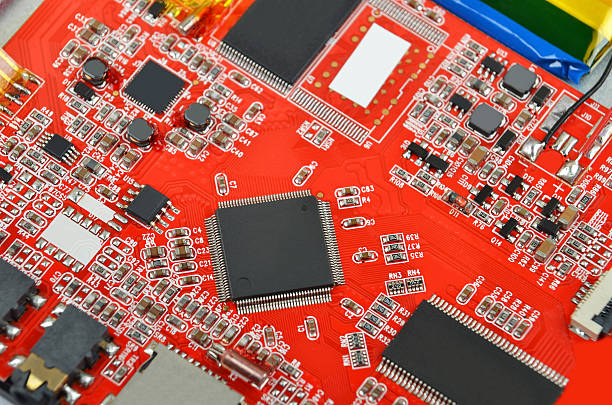
At the center of this hardware is the printed circuit board. A well-designed and properly manufactured access control PCB provides the electrical foundation for communication, identification, power management, and control functions.
Because access control equipment may operate continuously in offices, residential buildings, commercial facilities, and outdoor entrances, its PCB must provide stable electrical performance, environmental resistance, mechanical reliability, and consistent manufacturing quality.
This article explains the key requirements, manufacturing processes, testing methods, and quality considerations involved in producing reliable PCBs for smart access control systems.
1. Key Requirements for Access Control PCB Manufacturing
The operating environment and functional requirements of smart access control equipment determine the performance requirements of its PCB.
Stable Signal Transmission
Access control systems process identification data, communication signals, sensor inputs, and control commands in real time. The PCB must provide reliable signal paths and appropriate electrical characteristics to minimize signal loss, interference, and communication errors.
For higher-speed or more sensitive designs, controlled impedance, proper grounding, suitable layer stack-up, and careful routing may be required.
Environmental Reliability
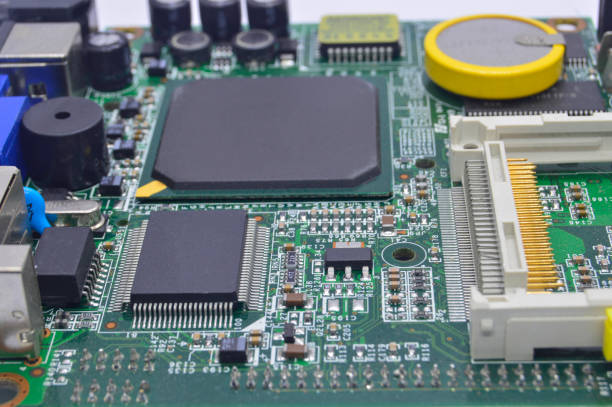
Access control equipment can be exposed to temperature fluctuations, humidity, dust, and repeated daily operation. Outdoor installations may face even more demanding conditions.
PCB materials, surface finishes, solder mask systems, and manufacturing processes should therefore be selected according to the expected operating environment.
Compact Mechanical Design
Many smart access control devices are designed with compact housings. The PCB must fit precisely inside the enclosure while maintaining appropriate clearances between components, connectors, mounting holes, and mechanical structures.
Dimensional accuracy is particularly important when the PCB must interface with displays, card readers, cameras, sensors, locks, communication modules, or other assemblies.
For projects requiring professional engineering support before fabrication, GOPCBA provides PCB Design & Layout services to help optimize designs for manufacturing and assembly.
2. Material Selection for Smart Access Control PCBs
Material selection establishes the foundation for PCB electrical and mechanical performance.
Choosing the Appropriate Laminate
FR-4 remains a common choice for many access control applications because it offers a practical balance of electrical insulation, mechanical strength, thermal resistance, and cost.
For designs with more demanding signal integrity requirements, a low-loss laminate may be considered to reduce dielectric losses and improve high-speed signal performance.
The correct material should be selected according to the operating frequency, thermal requirements, mechanical structure, layer count, and expected environment rather than simply choosing the lowest-cost option.
Copper Foil Selection
Copper is responsible for carrying current and electrical signals through the PCB.
Appropriate copper thickness should be selected based on current requirements, trace dimensions, thermal considerations, and manufacturing constraints. Consistent copper quality also helps improve electrical stability and manufacturing reliability.
Solder Mask and Silkscreen
The solder mask protects exposed copper from contamination and helps reduce the risk of unintended electrical contact.
For access control equipment expected to operate for long periods, the solder mask should provide suitable resistance to aging, handling, and environmental exposure.
Silkscreen markings should remain clear enough to support assembly, inspection, troubleshooting, and maintenance.
3. Key PCB Manufacturing Processes
A reliable PCB manufacturing process requires precise control across multiple production stages.
3.1 Circuit Pattern Formation
Circuit fabrication typically involves several important steps, including dry-film application, exposure, development, and etching.
The objective is to accurately reproduce the designed circuit pattern while maintaining the specified trace width and spacing.
For access control boards containing multiple functional modules, appropriate routing density and electrical separation are important. Excessively narrow spacing or uncontrolled etching can increase the risk of shorts, open circuits, and signal integrity problems.
Etching parameters must therefore be carefully controlled to maintain consistent line geometry and minimize defects such as undercutting, over-etching, and rough edges.
3.2 Lamination for Multilayer Boards
When an access control product requires a multilayer PCB, lamination becomes a critical manufacturing stage.
Inner layers are aligned according to the designed stack-up and bonded with prepreg under controlled temperature and pressure.
The lamination process must provide:
- Accurate layer registration
- Strong interlayer bonding
- Consistent dielectric thickness
- Minimal voids
- Low risk of delamination
- Good dimensional stability
Temperature, pressure, heating rate, curing time, and cooling conditions should be controlled according to the materials and board construction.
For more complex multilayer structures, professional PCB Manufacturing capabilities can help maintain consistency from prototype production through larger production runs.
3.3 Surface Finishing
The PCB surface finish affects solderability, corrosion resistance, contact reliability, and compatibility with downstream assembly processes.
Depending on the application, manufacturers may use finishes such as HASL, ENIG, or other suitable technologies.
ENIG, for example, can be useful when a board requires a relatively flat surface, good solderability, and reliable contact performance for connectors or other exposed interfaces.
The selected finish should be matched to the actual application rather than treated as a universal solution.
After surface treatment, inspection should verify appearance, coverage, thickness where applicable, and the absence of defects such as exposed copper, pits, or incomplete plating.
4. Quality Inspection for Access Control PCBs
Manufacturing quality should be verified through multiple inspection stages rather than relying solely on final visual inspection.
4.1 Visual and AOI Inspection
Visual inspection can identify obvious defects such as:
- Scratches
- Contamination
- Damaged board edges
- Solder mask defects
- Silkscreen problems
- Surface abnormalities
Automated Optical Inspection (AOI) can provide additional inspection of circuit patterns and identify defects such as missing features, abnormal trace geometry, shorts, and other manufacturing deviations.
Combining automated inspection with appropriate manual verification provides a more comprehensive quality-control approach.
4.2 Electrical Testing
Electrical testing is essential for verifying PCB functionality.
Depending on the board design and production stage, testing may include:
- Continuity testing
- Insulation resistance testing
- Flying probe testing
- Fixture-based testing
- Impedance verification
- Functional testing
For communication-intensive access control systems, additional signal integrity evaluation may be appropriate when required by the design.
The goal is to confirm that electrical paths conform to the design and that the PCB can reliably support the intended system functions.
4.3 Environmental Reliability Testing
Some access control PCB projects require additional reliability testing to evaluate performance under environmental stress.
Potential tests include:
- High-temperature storage
- Low-temperature storage
- Temperature cycling
- Damp heat testing
- Vibration testing
- Thermal stress testing
After environmental testing, the PCB should be inspected again to identify changes in appearance, electrical performance, dimensional stability, or structural integrity.
The exact testing requirements should be established according to the product’s operating environment and applicable industry standards.
5. How High-Quality PCBs Improve Access Control System Performance
A properly manufactured PCB can provide several important benefits to the finished access control product.
Improved Operational Stability
Reliable PCB construction helps maintain stable communication between identification modules, controllers, sensors, displays, and other electronic components.
This can reduce failures caused by poor electrical connections, environmental degradation, or manufacturing defects.
Support for Functional Expansion
As access control systems evolve, products may add features such as wireless communication, biometric recognition, touch interfaces, network connectivity, remote management, and additional sensors.
A high-density PCB design can integrate more functionality within a compact form factor while maintaining appropriate electrical and mechanical requirements.
This makes PCB engineering an important part of product development rather than simply a downstream manufacturing task.
Enhanced System Safety
Access control equipment is part of a security system, so reliable hardware is essential.
Proper insulation, trace spacing, grounding, electrical testing, and manufacturing quality can help reduce risks associated with short circuits, leakage, intermittent connections, or communication failures.
6. Important Considerations When Manufacturing Access Control PCBs
Establish Standardized Manufacturing Procedures
A standardized production process helps reduce variation between batches.
Manufacturers should define documented requirements for circuit fabrication, drilling, plating, lamination, surface finishing, inspection, and testing.
Process parameters should also be monitored and reviewed regularly to identify potential sources of variation.
Strengthen Supply Chain Management
Consistent material quality is essential for consistent PCB production.
A reliable PCB supplier should have effective controls for laminate, copper foil, solder mask, prepreg, surface-finish chemicals, and other production materials.
Incoming material inspection can help prevent unsuitable materials from entering the production process.
Supplier evaluation and traceability are also valuable for long-term production stability.
Use Automation Where Appropriate
Automation can improve manufacturing consistency and reduce operator-dependent variation.
Automated systems can support processes such as:
- Dry-film application
- Imaging and exposure
- Lamination
- Optical inspection
- Electrical testing
- Dimensional inspection
However, automation should complement rather than replace engineering process control. Equipment calibration, maintenance, programming, and process verification remain essential.
7. PCB Assembly Considerations for Smart Access Control Products
PCB fabrication is only one part of the manufacturing process. Once the bare board is completed, component placement and soldering also influence the final reliability of the access control product.
Components such as microcontrollers, communication modules, sensors, connectors, memory devices, power-management components, and interface devices must be assembled accurately.
A professional PCB Assembly process can integrate SMT and through-hole assembly according to the product’s requirements.
For new access control products, prototype production is especially valuable because it allows engineering teams to verify component placement, mechanical fit, electrical functionality, and assembly performance before committing to larger production quantities.
8. From Prototype to Production: Building a Reliable Manufacturing Workflow
A successful access control PCB project should connect design, fabrication, assembly, testing, and production planning into one coordinated workflow.
A typical development path may include:
- PCB design and engineering review
- Material and stack-up selection
- Prototype PCB fabrication
- Component procurement
- Prototype assembly
- Electrical and functional testing
- Design optimization
- Low-volume production
- Production validation
- Scaled manufacturing
This approach allows potential problems to be identified earlier and reduces the risk of transferring unresolved design or manufacturing issues into mass production.
For customers validating a new product, Prototype PCB Assembly provides a practical way to evaluate assembly and product performance before moving into larger-scale production.
Conclusion
Smart access control PCB manufacturing is a comprehensive engineering process involving material selection, circuit fabrication, multilayer lamination, surface finishing, inspection, electrical testing, and reliability verification.
Because access control systems must operate accurately and consistently, PCB quality directly affects the stability, functionality, and long-term reliability of the finished product.
A robust manufacturing strategy should therefore focus on more than individual production steps. Material quality, process standardization, equipment control, automated inspection, electrical testing, environmental reliability, and supply chain management all contribute to the final result.
As smart security systems become more connected, compact, and feature-rich, their PCB requirements will continue to evolve. Choosing an experienced PCB supplier with integrated engineering, fabrication, assembly, and testing capabilities can help product developers move from prototype to production with greater confidence.