Communication Test Equipment PCB: Key Requirements for High-Precision and High-Reliability Manufacturing
SEO Title: Communication Test Equipment PCB: Manufacturing Requirements and Quality Control
Meta Description: Explore the key requirements for communication test equipment PCBs, including high-frequency signal integrity, material selection, impedance control, advanced manufacturing, and quality testing.
Core Keywords: communication test equipment PCB, high-frequency PCB, PCB manufacturing, PCB quality control, PCB supplier
Communication test equipment plays an essential role in measuring and analyzing modern communication signals. From frequency and amplitude measurements to phase analysis and signal integrity verification, these instruments require highly reliable electronic hardware to deliver accurate results.
At the center of this hardware is the communication test equipment PCB. It connects functional modules, provides stable signal transmission, supports high-frequency circuits, and helps maintain consistent instrument performance over long operating periods.
As communication technologies move toward higher frequencies, faster data rates, and increasingly compact equipment, PCB manufacturers must pay close attention to material selection, impedance control, manufacturing precision, inspection technology, and process consistency.
1. Key Requirements for Communication Test Equipment PCBs
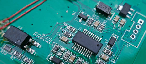
Communication test instruments place higher demands on PCB performance than many conventional electronic products. A suitable PCB must provide both electrical precision and long-term reliability.
High-Frequency Signal Integrity
Communication test equipment often handles high-frequency signals where even small impedance variations, transmission losses, or electromagnetic interference can affect measurement accuracy.
The PCB design and manufacturing process should therefore control:
- Controlled impedance
- Trace width and spacing
- Dielectric characteristics
- Signal return paths
- Crosstalk
- Transmission loss
- Via structures
- Grounding and shielding
For applications involving demanding high-speed or RF signals, selecting an appropriate high-frequency material and maintaining consistent manufacturing parameters are particularly important.
GOPCBA provides professional PCB Design & Layout services to help engineers consider manufacturability, signal integrity, component placement, routing, and other design requirements before production.
Long-Term Operating Stability
Communication test equipment may operate continuously for extended periods. The PCB must therefore maintain stable electrical and mechanical performance throughout its service life.
Important considerations include:
- Thermal stability
- Insulation performance
- Copper adhesion
- Surface finish reliability
- Resistance to humidity and temperature changes
- Mechanical strength
- Consistent electrical characteristics
A reliable communication test equipment PCB should not only pass initial electrical testing but also maintain predictable performance under actual operating conditions.
Compact and Scalable Design
Modern test instruments increasingly integrate more functions into smaller enclosures. This creates greater PCB density while leaving less physical space for routing and thermal management.
Multilayer construction, fine-line routing, controlled impedance structures, and appropriate via technologies can help manufacturers achieve higher circuit density without sacrificing reliability.
2. Material Selection Is the Foundation of PCB Performance
The material system has a direct influence on signal integrity, thermal behavior, mechanical stability, and manufacturing reliability.
High-Frequency PCB Materials
For demanding RF and high-speed applications, conventional FR-4 may not always provide the electrical characteristics required by the application. Depending on frequency and performance requirements, engineers may consider low-loss or high-frequency laminate systems.
Important material parameters include:
- Dielectric constant (Dk)
- Dissipation factor (Df)
- Thermal stability
- Dimensional stability
- Copper adhesion
- Moisture resistance
- Frequency-dependent electrical performance
The material should be selected according to the actual frequency range, impedance requirements, environmental conditions, and overall system architecture rather than simply choosing the most expensive option.
Copper Foil and Auxiliary Materials
Copper quality also affects conductor resistance and signal performance. Consistent copper thickness and strong copper adhesion are important for maintaining predictable electrical characteristics.
Other materials, including dry film, solder mask, bonding materials, and surface-finish chemicals, should also be controlled carefully. Inconsistent auxiliary materials can introduce defects even when the base laminate itself meets specifications.
A capable PCB supplier should establish incoming material inspection procedures and maintain traceability throughout production.
3. Precision PCB Manufacturing Processes
The manufacturing process must translate the electrical requirements defined during PCB design into a physically accurate and repeatable circuit structure.
GOPCBA supports PCB production from prototypes through volume manufacturing. Its PCB Manufacturing service covers different PCB technologies and production requirements, helping customers select an appropriate manufacturing solution based on board structure and application needs.
Precision Circuit Formation
Circuit formation requires accurate control of imaging, developing, etching, and related processes.
For high-density communication boards, manufacturers need to maintain tight control over:
- Minimum trace width
- Trace spacing
- Etching uniformity
- Line-edge quality
- Copper thickness
- Registration accuracy
Poor control can result in excessive etching, conductor-width variation, shorts, opens, or impedance deviations.
Multilayer Lamination
Many communication test instruments use multilayer PCBs to accommodate complex routing and dedicated power and ground structures.
During lamination, inner layers and dielectric materials are bonded under controlled temperature and pressure. Registration accuracy is particularly important because even small layer shifts can affect vias, signal traces, and impedance structures.
Lamination parameters should be established according to the selected material system and board construction. Heating rate, pressure profile, curing time, and cooling conditions all require appropriate control.
Surface Finishing
Surface finish affects solderability, corrosion resistance, contact reliability, and long-term performance.
Depending on the application, manufacturers may use finishes such as:
- ENIG
- Immersion silver
- HASL
- Other application-specific finishes
For precision communication equipment, the selected finish should be evaluated based on component type, connector requirements, soldering process, environmental conditions, and expected service life.
4. Advanced Equipment Supports Manufacturing Precision
High-performance PCBs require more than basic fabrication equipment. Manufacturing and inspection systems must provide sufficient precision and repeatability.
Impedance Testing
Controlled impedance is one of the most important characteristics for many communication-related PCBs.
Impedance testing helps verify whether manufactured transmission lines match the design requirements. Proper testing can identify variations caused by trace dimensions, dielectric thickness, copper thickness, or material characteristics.
Maintaining impedance consistency helps reduce unwanted signal reflections and supports more predictable high-frequency performance.
Dimensional and Plating Inspection
Mechanical dimensions must remain within the customer’s specified tolerances to ensure that the PCB fits correctly inside the test instrument.
Plating inspection can also verify surface-finish characteristics, helping ensure reliable electrical contact and solderability.
Depending on board requirements, manufacturers may combine dimensional inspection with automated optical inspection, electrical testing, cross-section analysis, and other verification methods.
5. PCB Quality Control Should Cover the Entire Production Process
A strong PCB quality control system should not depend solely on final inspection. Quality needs to be built into every stage of manufacturing.
Incoming Material Inspection
Before production begins, materials should be checked against the approved specifications.
Typical checks may include:
- Material model
- Thickness
- Copper thickness
- Surface condition
- Certification documentation
- Storage conditions
- Batch information
Critical materials may require additional verification before being released to production.
In-Process Inspection
Manufacturing parameters should be monitored throughout production rather than waiting until the finished board is available.
Depending on the product, inspection may include:
- AOI
- Dimensional inspection
- Registration verification
- Copper thickness measurement
- Impedance testing
- Plating inspection
- Cross-section analysis
Early detection reduces the risk of defective boards progressing to later processes.
Final Electrical Testing
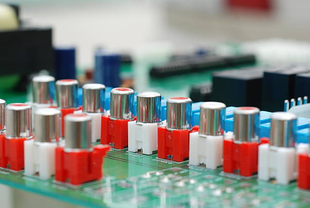
Electrical testing can verify continuity, isolation, and other customer-defined electrical characteristics.
For high-frequency communication applications, impedance and signal-related requirements may also need to be verified according to the engineering specification.
For customers who require assembled and tested products, GOPCBA also provides PCB Assembly services, integrating PCB fabrication and assembly requirements into a broader manufacturing workflow.
6. Engineering Capability Matters When Choosing a PCB Supplier
The quality of a communication PCB depends not only on equipment but also on engineering experience and process management.
A qualified PCB supplier should be able to evaluate a customer’s design before production and identify potential manufacturing risks.
Useful engineering support can include:
- DFM analysis
- Material selection
- Stack-up optimization
- Controlled impedance planning
- Manufacturing tolerance review
- Component availability assessment
- Prototype validation
- Production process optimization
For new communication equipment, prototype manufacturing is particularly valuable because it allows engineers to identify design and manufacturing problems before committing to larger production quantities.
GOPCBA’s Prototype PCB Assembly service can support early-stage product validation, while its Low Volume PCB Assembly service can help bridge the gap between prototypes and larger-scale production.
7. Why Manufacturing Consistency Is Critical for Communication Test Equipment
A communication test instrument is only as reliable as the hardware supporting its measurement chain.
If PCB characteristics vary significantly between production batches, the instrument may experience changes in signal behavior, calibration stability, or overall measurement consistency.
Manufacturers should therefore focus on repeatability in:
- Material selection
- PCB stack-up
- Circuit dimensions
- Lamination
- Copper plating
- Surface finishing
- Controlled impedance
- Electrical testing
- Production documentation
- Process traceability
This systematic approach helps ensure that prototype boards and production boards behave as consistently as possible.
Conclusion
A communication test equipment PCB must satisfy much more than basic electrical connectivity. It needs to support high-frequency signal integrity, accurate impedance characteristics, mechanical stability, thermal performance, and long-term reliability.
Achieving these requirements requires a combination of suitable materials, precision PCB manufacturing, advanced inspection equipment, disciplined process control, and comprehensive PCB quality control.
For communication test equipment developers, selecting an experienced PCB supplier early in the product-development process can reduce manufacturing risks, improve prototype validation, and create a smoother path from initial design to reliable production.