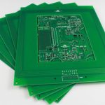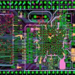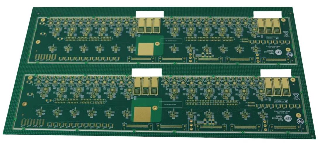
A printed circuit board (PCB) provides the electrical and mechanical foundation for electronic components. From simple single-sided boards to complex multilayer circuits, different production techniques can be used depending on the required precision, production volume, materials, and application.
Modern PCB Manufacturing typically relies on automated imaging, CNC drilling, laser processing, plating, etching, solder mask application, and automated inspection. However, traditional PCB production methods remain useful for prototyping, education, hobby projects, and understanding the fundamentals of PCB fabrication.
This article introduces several traditional PCB production methods and explains the basic principles behind them.
1. Traditional PCB Production Method: Wax-Paper Circuit Transfer
One traditional approach to PCB Production uses a manually prepared circuit pattern that is transferred onto a copper-clad board before etching.
Step 1: Prepare the Copper-Clad Laminate
Cut the copper-clad laminate to the required board dimensions.
The copper surface should be clean and free from oxidation, grease, dust, and other contaminants. Proper surface preparation is important because contamination can reduce the adhesion of the circuit pattern.
Step 2: Prepare the Circuit Pattern
Place wax paper over a steel plate and manually engrave the circuit pattern at a 1:1 scale.
The circuit pattern should correspond accurately to the final PCB dimensions. The prepared pattern can then be transferred onto the copper surface using an appropriate resist or printing material.
For small quantities, the same pattern can be reused to produce several boards.
Step 3: Etching
The exposed copper can be removed using a suitable PCB etching solution.
Historically, various chemical systems were used for this purpose. Modern PCB fabrication generally uses controlled industrial etching processes rather than manually prepared chemical mixtures.
When chemical etching is performed, the chemical concentration, temperature, exposure time, ventilation, and waste treatment must be properly controlled.
Step 4: Cleaning and Drilling
After etching, thoroughly rinse the board to remove residual etchant.
The temporary resist can then be removed using an appropriate solvent. After cleaning and drying, the board can be drilled according to the component and mounting-hole requirements.
A protective coating such as rosin may be applied to the finished copper surface in traditional hobbyist processes.
Safety Note: Chemical etching should be performed only with appropriate personal protective equipment, ventilation, chemical handling procedures, and waste disposal. Industrial PCB Manufacturing requires dedicated chemical-management and wastewater-treatment systems.
2. Traditional PCB Production Method: Transfer Film and Adhesive Tape
Another traditional method uses transfer pads and adhesive tape to manually construct the circuit pattern.
Step 1: Prepare the PCB Artwork
Create the circuit artwork based on the schematic and required PCB dimensions.
Pads can be represented as dots, while electrical connections are represented as lines. The artwork must maintain accurate dimensions and component spacing.
Step 2: Cut and Clean the Copper-Clad Board
Cut the copper-clad laminate to the required size.
Clean and lightly abrade the copper surface to remove oxidation and improve adhesion between the copper and the transfer material.
Step 3: Transfer the Circuit Pattern
The circuit drawing can be transferred to the copper surface using carbon paper or another suitable transfer technique.
For simple circuits, experienced technicians may construct the pattern directly without this intermediate transfer step.
Step 4: Apply Transfer Pads and Tape
Different pre-cut transfer pads can be selected according to the required component-hole dimensions.
Adhesive tape can then be used to represent PCB traces. Different tape widths can be selected according to the expected current and electrical requirements.
Traditional transfer materials were available in various sizes, but modern PCB design software and photolithographic imaging have largely replaced this manual approach.
Step 5: Secure the Transfer Pattern
Use a soft tool to gently press the transfer pads and adhesive traces onto the copper surface.
Special attention should be given to corners, intersections, and narrow features because poorly adhered transfer material can cause incomplete or irregular etching.
Gentle heating may be used with appropriate materials to improve adhesion, provided that the material manufacturer’s temperature limits are followed.
Step 6: Etch the PCB
Place the board into an appropriate etching solution and carefully control the etching conditions.
The etching process should be monitored to prevent excessive undercutting of narrow traces.
After etching is complete, rinse the board thoroughly and remove the remaining transfer material.
Step 7: Drill and Finish
Drill component and mounting holes according to the PCB design.
The copper surface can then be cleaned and finished with an appropriate protective coating.
Although this method can produce functional prototype boards, its dimensional accuracy and repeatability are significantly lower than those achieved by modern PCB Fabrication processes.
3. Traditional PCB Production Method: Hand-Drawn Resist
A third method uses a manually prepared protective coating to draw the circuit pattern directly onto a copper-clad board.
Historically, shellac-based or other resist materials were dissolved in alcohol and used as a protective coating. A small amount of coloring agent could be added to make the coating easier to see.
Step 1: Prepare the Copper Surface
Lightly polish the copper surface using fine abrasive material.
The surface should then be cleaned thoroughly to remove dust, grease, and oxidation.
Step 2: Draw the Circuit
A drawing pen or technical pen can be used to apply the resist directly to the copper surface.
A ruler, set square, or other precision drawing tool can help create straight and consistent lines.
The line width should be controlled according to the required circuit geometry.
If the resist spreads into the surrounding area, it may be too thin. If the pen cannot move smoothly, the resist may be too thick.
Step 3: Correct the Pattern
Errors can be removed using a suitable solvent and then redrawn.
The circuit pattern should be carefully inspected before etching because any gap in the resist can expose copper that should remain in the final circuit.
Step 4: Etch the Board
Once the resist pattern is complete, the board can be etched using an appropriate PCB etchant.
After etching, the remaining resist can be removed with a compatible solvent.
The board should then be cleaned, dried, and inspected before drilling and assembly.
Limitations of Hand-Drawn PCB Fabrication
This method is suitable primarily for simple prototype circuits.
It is not recommended for:
- Fine-pitch components
- High-density interconnects
- Controlled-impedance circuits
- High-speed PCB designs
- Multilayer boards
- High-volume production
Modern PCB Manufacturing Process technologies provide substantially better dimensional accuracy, repeatability, and production efficiency.
4. Traditional PCB Production Method: Adhesive Copper Foil
Another simple approach is to apply copper foil or adhesive material to the surface of a copper-clad board and manually remove the unwanted areas.
Step 1: Apply the Copper Foil
Apply the adhesive copper material evenly to the required area of the board.
The material should be firmly attached without wrinkles or air bubbles.
Step 2: Cut the Circuit Pattern
Use a precision cutting tool to remove the portions that do not belong to the circuit.
The remaining copper pattern forms the desired conductive traces.
Step 3: Etch the Board
The exposed copper can then be removed through chemical etching.
An elevated etching temperature may increase the etching rate, but the actual operating temperature should be controlled according to the specific chemical system and safety requirements.
After etching, rinse the board thoroughly and remove the remaining adhesive material.
Step 4: Drill and Finish
Drill the required component holes and mounting holes.
The finished board can then be cleaned and protected with an appropriate surface coating.
This technique is relatively simple but has limited precision and is therefore mainly suitable for basic prototypes and educational applications.
5. PCB Layout Preparation Before Fabrication
Before beginning PCB Fabrication, the circuit should first be converted into a suitable physical layout.
5.1 Component Placement
Components should be arranged according to the electrical schematic, mechanical constraints, board dimensions, and assembly requirements.
A practical placement strategy is:
- Place large or mechanically constrained components first.
- Position connectors and mounting hardware.
- Arrange major functional blocks.
- Place smaller components around their associated devices.
- Optimize component orientation and spacing.
- Verify assembly and maintenance requirements.
Components belonging to the same electrical function should generally be placed close together where appropriate.
5.2 PCB Routing
Connections between components should be routed carefully to minimize unnecessary trace length and avoid unwanted interference.
For modern PCB Design, routing should consider:
- Trace width
- Trace spacing
- Current capacity
- Signal integrity
- Return-current paths
- Crosstalk
- Electromagnetic interference
- Thermal requirements
- Manufacturing capability
Sharp 90-degree corners should generally be avoided, particularly in high-speed designs. Smooth 45-degree routing or curved transitions are preferred where appropriate.
5.3 Input and Output Separation
Input and output circuits should be physically separated where possible to reduce unwanted coupling and feedback.
Sensitive analog signals should also be separated from noisy digital, switching, or high-current circuits when required by the application.
For modern high-speed PCB designs, placement and routing should be determined based on signal integrity and electromagnetic compatibility requirements rather than relying solely on traditional routing rules.
6. Traditional PCB Production Method: Screen Printing
Screen printing is another traditional method that can be used to transfer PCB artwork onto a copper-clad laminate.
Step 1: Prepare the Artwork
Print the PCB artwork at a 1:1 scale onto suitable transparent or semi-transparent film.
The artwork should be dimensionally accurate and properly aligned.
Step 2: Prepare the Screen
A screen-printing frame can be prepared with a suitable mesh.
The artwork film is positioned accurately against the screen so that the desired circuit pattern can be transferred.
Step 3: Position the Copper-Clad Board
Place the prepared screen over the copper-clad board.
The board and screen must remain properly aligned throughout the printing process.
Step 4: Apply the Resist
Apply a suitable PCB resist to the screen.
Use a controlled, consistent motion to transfer the resist through the mesh onto the copper surface.
The amount of pressure and resist applied should be controlled carefully.
If too much resist is applied, the circuit features may become wider than intended. If too little resist is applied, traces may become discontinuous.
Step 5: Dry and Inspect
Allow the printed resist to dry or cure according to the material requirements.
Inspect the circuit pattern for:
- Broken traces
- Pinholes
- Excess resist
- Smearing
- Misalignment
- Incomplete coverage
Minor defects may be corrected manually for prototype applications.
Step 6: Etching
After the resist has been properly prepared, the exposed copper can be removed using a suitable etching process.
The board should then be thoroughly cleaned and inspected.
Step 7: Printing Component Information
The same general screen-printing principle can be used to create component markings and other PCB identification information.
Modern PCB factories normally use dedicated imaging and silkscreen processes to achieve much higher accuracy and consistency.
7. Modern PCB Manufacturing Process
Although the traditional methods above are useful for understanding the fundamentals of PCB fabrication, commercial PCB production has evolved significantly.
A typical modern PCB Manufacturing Process may include the following stages:
7.1 Engineering and DFM Review
Before production begins, the PCB design data is reviewed for manufacturability.
The DFM review checks items such as:
- Minimum trace width
- Minimum spacing
- Hole diameter
- Annular ring
- Copper thickness
- Board thickness
- Solder mask clearance
- Silkscreen clearance
- Board outline
- V-CUT and routing requirements
7.2 Imaging
Modern PCB factories use photolithography or direct imaging to transfer circuit patterns onto the copper surface.
This provides substantially greater accuracy than manually drawn or transferred artwork.
7.3 Etching
Unwanted copper is removed through a controlled industrial etching process.
Process parameters are carefully controlled to maintain the required trace width and spacing.
7.4 Drilling
CNC drilling is used for conventional through-holes.
For high-density boards, laser drilling may be used to produce microvias and other fine features.
7.5 Plating
Copper plating is used to create electrical connections between PCB layers and to build up the required copper thickness on plated holes and circuit features.
7.6 Solder Mask
A solder mask coating is applied to protect copper traces and prevent solder bridges during assembly.
7.7 Surface Finish
Depending on the application, common PCB surface finishes include:
- HASL
- Lead-free HASL
- ENIG
- OSP
- Immersion tin
- Immersion silver
The appropriate surface finish depends on component pitch, soldering method, reliability requirements, environmental regulations, and cost.
7.8 Electrical Testing and Inspection
Finished PCBs may undergo automated optical inspection (AOI), electrical testing, dimensional inspection, solder mask inspection, and other quality-control procedures.
These processes help identify open circuits, short circuits, missing features, dimensional problems, and other manufacturing defects.
8. Traditional vs. Modern PCB Manufacturing
Traditional PCB production methods are useful for prototypes and learning because they require relatively simple tools and processes.
However, they have significant limitations compared with modern PCB Manufacturing.
| Feature | Traditional Methods | Modern PCB Manufacturing |
|---|---|---|
| Circuit transfer | Manual or screen printing | Photolithography / direct imaging |
| Trace accuracy | Relatively low | High |
| Repeatability | Limited | High |
| Minimum feature size | Relatively large | Much smaller |
| Hole processing | Manual drilling | CNC / laser drilling |
| Multilayer capability | Very limited | Highly developed |
| Quality control | Mostly manual | Automated inspection and testing |
| Production volume | Small | Prototype to mass production |
| Cost efficiency | Suitable for simple prototypes | Better for commercial production |
| Process control | Operator dependent | Automated and monitored |
The choice of manufacturing technology should therefore be based on the PCB’s complexity, production volume, electrical requirements, mechanical requirements, and target cost.
9. How to Choose the Right PCB Production Method
When selecting a PCB Production method, consider the following factors:
Prototype or Hobby Project
Traditional transfer, hand-drawn, or screen-printing techniques may be sufficient for simple circuits.
Professional Prototype
For functional engineering prototypes, commercial PCB fabrication is generally preferable because it provides better dimensional accuracy, hole quality, solder mask performance, and electrical reliability.
High-Density PCB
Fine-pitch components, HDI structures, microvias, and multilayer designs require advanced manufacturing equipment and controlled processes.
High-Volume Production
Mass production requires stable processes, automated inspection, controlled material handling, high repeatability, and efficient production equipment.
10. Conclusion
PCB production technology has developed from simple manual techniques into a highly automated manufacturing process.
Traditional methods such as wax-paper transfer, adhesive tape, hand-drawn resist, copper foil cutting, and screen printing can help explain the fundamental principles of circuit pattern transfer and copper etching. They may still be useful for simple prototypes, education, and hobby projects.
However, modern PCB Fabrication requires much higher levels of precision and process control. Professional PCB manufacturers use DFM analysis, automated imaging, CNC drilling, copper plating, controlled etching, solder mask processing, surface finishing, AOI, and electrical testing to achieve consistent production quality.
For commercial PCB projects, designers should consider manufacturing requirements from the beginning of the PCB Design process. Early DFM communication with the manufacturer can reduce redesigns, improve production yield, shorten lead time, and control manufacturing costs.
Kingda can work with customers during the design and engineering stage to evaluate PCB manufacturability and recommend suitable production processes based on board structure, materials, feature dimensions, and application requirements.