Why Does PCB Impedance Control? | Controlled Impedance PCB
A PCB can be regarded as a high-speed pathway for electrical signals, and its electrical characteristics directly influence the stability, response speed, and reliability of an electronic system. As data rates and operating frequencies continue to increase, PCB Impedance Control has become an important part of modern PCB design and manufacturing.
Impedance control is particularly important for high-speed digital, RF, microwave, networking, telecommunications, automotive, and other signal-sensitive applications. It connects PCB geometry, dielectric materials, stack-up design, and manufacturing tolerances with the electrical requirements of the complete system.
Understanding why impedance control matters requires looking at three key areas: signal transmission, application requirements, and manufacturing control.
Why Is PCB Impedance Control Important?
Impedance Matching for Reliable Signal Transmission
When an electrical signal travels through a PCB transmission line, its behavior depends on the physical structure and electrical properties of the transmission path. Unlike simple DC resistance, characteristic impedance describes how a transmission line responds as a signal propagates through the PCB.
When a signal encounters an impedance discontinuity, part of its energy can be reflected toward the source. These reflections can interfere with the original signal and create problems such as signal distortion, ringing, overshoot, undershoot, timing errors, and reduced signal margins.
For this reason, Controlled Impedance PCB manufacturing aims to maintain predictable transmission-line characteristics throughout the signal path.
The characteristic impedance of a PCB trace is influenced by several factors, including:
- Trace width
- Copper thickness
- Dielectric thickness
- Dielectric constant
- Distance to the reference plane
- Trace geometry
- Copper surface characteristics
- PCB stack-up
- Manufacturing tolerances
A stable combination of these parameters helps the finished board achieve the impedance specified by the electrical design.
Impedance and Signal Integrity
For a High-Speed PCB, impedance control is closely connected with signal integrity.
As signal rise times become faster, PCB traces increasingly behave as transmission lines. Even when the nominal clock frequency does not appear extremely high, fast signal transitions can make impedance discontinuities significant.
Poor impedance control can contribute to:
- Signal reflection
- Waveform distortion
- Timing uncertainty
- Crosstalk
- Electromagnetic interference
- Reduced signal-to-noise margin
- Data transmission errors
- Communication instability
Therefore, impedance should not be treated simply as a final testing requirement. It should be considered during stack-up development, material selection, routing, and manufacturing engineering.
Which Applications Require Impedance Control?
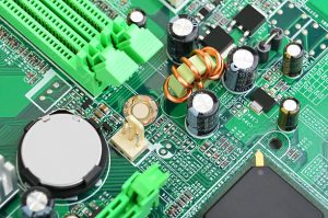
As electronic products move toward higher frequencies, faster data rates, and greater integration, impedance control has become essential for a growing range of applications.
Telecommunications and Networking Equipment
5G base stations, network switches, routers, optical communication equipment, and other telecommunications hardware often contain high-speed digital and RF signal paths.
In these applications, impedance variations can affect transmission performance and signal quality. RF circuits may be particularly sensitive to impedance mismatches because they can influence signal reflection, insertion loss, and power transfer.
GOPCBA provides High-Frequency PCB Manufacturing solutions for applications requiring specialized materials, multilayer structures, and controlled impedance.
Industrial Control and Medical Electronics
Industrial control systems and medical equipment often require stable and predictable signal transmission.
Signal disturbances can affect sensor readings, communication between control modules, or the accuracy of measurement systems. Proper impedance design and manufacturing can help establish a more predictable electrical environment for sensitive signal paths.
For these applications, impedance control should be considered together with grounding, shielding, stack-up structure, routing, and electromagnetic compatibility.
Consumer Electronics and High-Speed Interfaces
Smartphones, computers, displays, storage devices, and other consumer electronics increasingly rely on high-speed interfaces.
Differential interfaces and high-speed serial links require carefully controlled transmission-line geometry. Variations in trace width, spacing, dielectric thickness, or reference-plane configuration can affect differential impedance and signal quality.
A well-engineered High-Speed PCB therefore requires impedance targets to be established before critical routing is finalized.
Automotive Electronics
Modern vehicles contain numerous high-speed communication and sensing systems, including ADAS, radar, cameras, vehicle networking, control units, and other electronic modules.
Automotive electronics also operate under temperature changes, vibration, electrical noise, and long service cycles. Consequently, PCB impedance control must be combined with appropriate material selection, multilayer construction, thermal considerations, and manufacturing consistency.
GOPCBA’s Automotive Multilayer PCB Manufacturing solutions address advanced multilayer, HDI, high-frequency, and controlled-impedance PCB requirements for demanding automotive electronics.
How Is PCB Impedance Controlled During Manufacturing?
The target impedance of a PCB is determined by the interaction between the electrical design and the physical structure of the board.
Trace Width
Trace width is one of the fundamental parameters affecting characteristic impedance. Manufacturing variations caused by etching, plating, or process control can change the final trace geometry.
For controlled-impedance designs, the manufacturer must establish a practical trace-width process window that can be reproduced consistently.
Copper Thickness
Copper thickness affects the effective geometry of a transmission line. Finished copper thickness can differ from the nominal starting copper thickness because of plating and other manufacturing processes.
Therefore, copper thickness should be considered when calculating and validating the final impedance.
Copper surface roughness can also become important in high-frequency applications because rough conductive surfaces may increase conductor loss.
Dielectric Thickness
The distance between a signal trace and its reference plane has a significant influence on impedance.
If the dielectric thickness changes, the electrical relationship between the signal trace and reference plane also changes. Stable lamination and accurate dielectric construction are therefore essential for consistent impedance.
Dielectric Constant
The dielectric constant, or Dk, of the PCB material influences signal propagation and transmission-line impedance.
The effective Dk used for impedance calculations can depend on the material system, resin content, glass style, frequency, and measurement method. Therefore, actual manufacturer-supplied material data should be used when developing the final stack-up.
PCB Stack-Up
A properly engineered stack-up defines the relationship between signal layers, ground planes, power planes, and dielectric materials.
For controlled-impedance applications, stack-up design should be completed before critical routing is finalized. The selected stack-up must also be compatible with the manufacturer’s actual lamination and fabrication capabilities.
GOPCBA provides Multilayer PCB Manufacturing for complex multilayer and impedance-controlled PCB structures.
Impedance Control Starts Before PCB Manufacturing
A common mistake is to complete the PCB layout using theoretical material and stack-up parameters and only afterward ask the manufacturer to reproduce the design.
A more reliable process is to involve the PCB manufacturer during the engineering stage.
A typical workflow includes:
- Define the target impedance according to the interface and system requirements.
- Select appropriate PCB materials.
- Develop the PCB stack-up.
- Calculate trace width, spacing, and transmission-line geometry.
- Review the design for manufacturability.
- Confirm manufacturing tolerances.
- Fabricate the PCB using controlled processes.
- Perform impedance testing.
- Compare measured results with the specified target.
- Release the validated production lot.
This approach helps connect the electrical design with actual manufacturing conditions.
What Happens When Impedance Control Is Ignored?
Failure to control impedance can create a range of problems depending on the signal speed, frequency, interface, and system architecture.
Signal Reflection
When impedance changes along a transmission path, part of the signal can be reflected. The resulting interference can distort the waveform received by the device.
Signal Distortion
Reflections and transmission-line discontinuities can produce ringing, overshoot, undershoot, and other waveform abnormalities.
Timing Errors
In high-speed digital systems, signal distortion can reduce timing margins and make it more difficult for receivers to distinguish valid logic states.
Crosstalk and EMI
Poor routing geometry and impedance discontinuities can contribute to unwanted coupling between neighboring signal paths and may increase electromagnetic interference.
Communication Failures
In severe cases, signal-integrity problems can lead to intermittent communication, data corruption, link instability, or complete transmission failure.
The severity of these effects depends on the interface and system design, but the general principle is clear: as signal transitions become faster, maintaining predictable transmission-line characteristics becomes increasingly important.
How Is Impedance Verified?
Impedance control requires both process management and electrical verification.
During production, manufacturers can use test coupons designed to represent the electrical characteristics of the PCB. Depending on the project requirements, impedance may be measured using time-domain reflectometry or another appropriate measurement method.
The measured impedance should then be compared with the customer’s specified target and tolerance.
GOPCBA’s Controlled Impedance PCB Manufacturing approach combines stack-up engineering, material selection, manufacturing control, and impedance verification for high-speed and high-frequency applications.
Impedance Control for High-Speed and High-Frequency PCBs
The importance of impedance control becomes even more apparent in advanced electronic systems.
High-Speed Digital Circuits
High-speed interfaces use fast signal transitions and often rely on differential transmission lines. Maintaining consistent trace geometry and reference-plane relationships helps support reliable signal transmission.
RF and Microwave Circuits
RF and microwave circuits can be highly sensitive to impedance mismatch. Maintaining appropriate transmission-line characteristics is essential for controlling reflection and transmission loss.
Differential Pairs
Differential impedance depends not only on individual trace dimensions but also on the spacing and coupling between the two conductors.
Changes in differential-pair spacing can alter coupling and therefore affect the final differential impedance.
HDI and Dense Multilayer Structures
HDI and high-density multilayer designs introduce additional considerations such as microvias, blind vias, buried vias, via transitions, and sequential lamination.
These structures can create localized impedance discontinuities if not properly engineered. Therefore, impedance analysis should include the complete signal path rather than only the straight portions of the traces.
PCB Impedance Control and Manufacturing Quality
Impedance control is not an isolated manufacturing operation. It depends on the consistency of multiple PCB fabrication processes.
Important manufacturing factors include:
- Material consistency
- Inner-layer circuit formation
- Etching accuracy
- Copper thickness
- Lamination control
- Dielectric thickness
- Layer registration
- Drilling accuracy
- Plating
- Surface treatment
- Impedance testing
- Final inspection
A small deviation in one parameter may influence the electrical characteristics of the finished PCB.
For this reason, experienced PCB manufacturers should evaluate impedance requirements from both electrical and manufacturing perspectives.
Why Choose GOPCBA for Controlled Impedance PCB Manufacturing?
GOPCBA provides PCB manufacturing solutions for high-speed, high-frequency, multilayer, HDI, and controlled-impedance applications.
Its manufacturing approach integrates material selection, stack-up engineering, DFM review, precision fabrication, impedance control, testing, and production support.
For demanding electronic applications, GOPCBA supports technologies including:
- Controlled-impedance PCB manufacturing
- High-speed PCB manufacturing
- High-frequency PCB manufacturing
- Multilayer PCB fabrication
- HDI PCB technology
- Blind and buried vias
- High-layer-count PCB structures
- PCB prototyping
- PCB assembly
- Production manufacturing
GOPCBA also supports PCB Design & Layout Services for projects where stack-up, routing, impedance, and manufacturing feasibility need to be considered together.
Conclusion
PCB impedance control is essential whenever signal integrity becomes a critical factor in electronic system performance.
The purpose of impedance control is not simply to achieve a specific numerical value. It is to create a predictable transmission path in which trace geometry, copper thickness, dielectric properties, stack-up configuration, and manufacturing tolerances work together to meet the electrical requirements of the application.
For high-speed digital, RF, telecommunications, automotive, industrial, medical, and other advanced electronic systems, proper impedance control can help reduce signal reflection, waveform distortion, timing errors, crosstalk, EMI, and transmission failures.
As electronic products continue to move toward higher data rates and frequencies, cooperation between PCB designers and manufacturers becomes increasingly important. A PCB supplier with strong engineering capabilities, material knowledge, precision manufacturing processes, and impedance testing capability can provide a more reliable foundation for high-performance electronic systems.
GOPCBA provides advanced PCB manufacturing and assembly solutions for high-speed, high-frequency, multilayer, HDI, and controlled-impedance applications, supporting projects from prototype development through production.