High-Frequency Multilayer PCB Customization
In 5G communications, satellite navigation, radar systems, high-speed servers, and other advanced electronic applications, stable high-frequency signal transmission is essential for system performance. A High-Frequency Multilayer PCB provides the electrical platform required to transmit high-frequency signals while maintaining signal integrity, transmission efficiency, and operational stability.
Compared with conventional PCBs, high-frequency multilayer boards require much greater attention to material selection, stack-up design, impedance control, fabrication tolerances, and testing. Each manufacturing parameter can affect electrical performance, making customized engineering essential for different operating frequencies and application requirements.
GOPCBA provides High-Frequency PCB Manufacturing solutions covering high-frequency materials, multilayer structures, controlled impedance, HDI, and other advanced PCB technologies, supporting projects from prototype development to production.
Material Selection for High-Frequency Multilayer PCBs
The foundation of a reliable High-Frequency Multilayer PCB is appropriate material selection. Unlike conventional PCBs that commonly use standard FR-4, high-frequency applications may require laminates with controlled dielectric constant and low dielectric loss.
The material should be selected according to:
- Operating frequency and bandwidth
- Dielectric constant (Dk)
- Dissipation factor (Df)
- Thermal requirements
- Mechanical requirements
- Layer structure
- Cost and production volume
High-performance RF materials, low-loss laminates, and high-Tg materials may be considered depending on the application. For demanding RF applications, material systems from manufacturers such as Rogers, Taconic, Isola, Panasonic, and other specialized laminate suppliers may be evaluated according to the required electrical characteristics.
Copper selection is also important. Low-profile copper can help reduce conductor loss at high frequencies because surface roughness can influence signal propagation and increase high-frequency loss.
For projects requiring different PCB structures and materials, PCB Manufacturing provides access to multilayer, high-frequency, high-speed, HDI, rigid-flex, heavy-copper, and other advanced PCB fabrication technologies.
Precision Manufacturing Process for High-Frequency PCBs
Manufacturing precision is a critical part of High-Frequency PCB Manufacturing. At high frequencies, relatively small variations in trace geometry, dielectric thickness, layer registration, or material characteristics can affect impedance and signal integrity.
Multilayer Stack-Up Design
The stack-up forms the physical foundation of a multilayer PCB. During customization, engineers must determine the number of layers, signal layers, ground planes, power planes, dielectric thicknesses, and copper thicknesses according to the electrical requirements.
For complex designs, a pure high-frequency stack-up or hybrid stack-up can be selected.
Hybrid constructions can combine high-frequency laminates with conventional PCB materials, potentially balancing electrical performance and manufacturing cost. However, different materials may have different thermal expansion characteristics and lamination behavior, so the stack-up must be engineered carefully to reduce warpage, delamination, and registration problems.
For high-speed designs, High-Speed PCB Lamination also requires careful control of dielectric thickness, layer position, material characteristics, and impedance requirements.
Precision Drilling and Via Metallization
Drilling and via metallization directly affect the electrical continuity and mechanical reliability of a multilayer PCB.
High-frequency vias should be designed with attention to parasitic capacitance and inductance. Drilling parameters must be matched to the selected laminate to minimize rough hole walls, burrs, breakout, and other defects.
After drilling, the hole walls must be properly prepared and metallized to establish reliable electrical connections between layers. Uniform copper deposition and appropriate plating control are particularly important for complex multilayer structures.
Advanced designs may also use blind vias, buried vias, or microvias to shorten interconnections and improve routing density.
High-Precision Circuit Formation
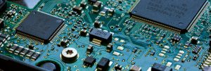
The circuit pattern directly affects high-frequency transmission performance. Trace width, spacing, copper thickness, and surface roughness all contribute to the electrical characteristics of the transmission line.
Fine-line fabrication may be required for compact high-frequency designs with dense routing. Advanced imaging technologies and tightly controlled processing conditions help maintain dimensional accuracy and reduce line-width variation.
Etching must also be carefully controlled. Excessive side etching or uneven conductor profiles can change the effective trace geometry and consequently affect impedance.
Surface finishing should be selected according to the electrical, assembly, and environmental requirements of the final application. A suitable surface finish can provide a stable interface while maintaining the required surface characteristics.
Controlled Impedance and Signal Integrity
One of the most important requirements of a Controlled Impedance PCB is maintaining predictable transmission-line characteristics throughout the manufacturing process.
Impedance depends on multiple factors, including:
- Trace width
- Trace thickness
- Dielectric thickness
- Dielectric constant
- Layer structure
- Copper surface characteristics
- Reference-plane configuration
For high-frequency and high-speed circuits, impedance targets must be established during the stack-up design stage rather than treated as a final inspection item.
Depending on the circuit, single-ended or differential impedance may be required. The actual target should be determined by the interface and system architecture.
GOPCBA’s high-speed PCB engineering approach includes stack-up review, impedance analysis, material selection, DFM review, and production verification.
Quality Control for High-Frequency Multilayer PCBs
Quality testing is the final verification stage of a customized High-Frequency Multilayer PCB. The inspection process should evaluate both structural integrity and electrical performance.
Structural Inspection
Structural inspection may verify:
- Layer registration
- Lamination quality
- Hole diameter and position
- Hole-wall copper
- Trace width and spacing
- Board thickness
- Surface finish
- Internal defects
For complex multilayer boards, cross-sectional analysis and X-ray inspection can provide additional information about internal structures.
Electrical Testing
Electrical testing verifies circuit connectivity and helps identify opens, shorts, and other electrical defects.
For controlled-impedance designs, test coupons and TDR measurements can be used to verify whether the manufactured transmission lines meet the specified impedance requirements. Production data such as impedance measurements, cross-section reports, thickness measurements, and registration results can provide objective evidence of process consistency.
Material Verification
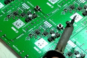
Material and copper specifications should also be controlled because changes in dielectric properties, copper thickness, or surface characteristics can affect high-frequency performance.
Material traceability and process control are especially important when the PCB is produced in multiple batches or transitions from prototype to mass production.
Applications of High-Frequency Multilayer PCBs
Demand for RF PCB and high-frequency multilayer technology continues to expand as electronic systems become faster, smaller, and more integrated.
Typical applications include:
- 5G communication equipment
- RF communication systems
- Radar systems
- Satellite navigation
- Aerospace electronics
- High-speed servers
- Data-center equipment
- Wireless communication devices
- Automotive radar
- Industrial sensing systems
For radar applications, for example, PCB designs may require low-loss materials, controlled impedance, RF routing, precision multilayer stack-ups, and specialized via technologies.
Customization Trends for High-Frequency Multilayer PCBs
As electronic systems continue to increase in frequency, speed, and integration density, high-frequency PCB customization is moving toward higher layer counts, lower transmission loss, tighter dimensional tolerances, and more sophisticated interconnection technologies.
HDI and microvia structures can increase routing density within compact designs. Low-loss materials can reduce signal attenuation, while controlled-impedance construction helps maintain predictable electrical performance.
At the same time, manufacturing consistency becomes increasingly important. A material and stack-up strategy that performs well during prototyping should ideally remain suitable as the project progresses from engineering validation to pilot production and mass production. This reduces the risk of redesign caused by material substitution or manufacturing changes.
Conclusion
Customized high-frequency multilayer PCB manufacturing is a coordinated process involving material selection, stack-up engineering, precision drilling, circuit formation, impedance control, lamination, and comprehensive testing.
The objective is not simply to manufacture a multilayer board, but to create a PCB structure that matches the application’s frequency, electrical performance, mechanical requirements, and production conditions.
By combining suitable high-frequency materials, controlled impedance, precision fabrication, advanced multilayer construction, and systematic quality control, a High-Frequency Multilayer PCB can provide stable signal transmission for demanding communication, radar, aerospace, server, and other high-performance electronic applications.
GOPCBA provides High-Frequency PCB Manufacturing and advanced Multilayer PCB fabrication capabilities, including high-speed, HDI, controlled-impedance, rigid-flex, high-TG, and high-layer-count PCB solutions.
For projects requiring both PCB fabrication and assembly, GOPCBA can also support the transition from prototype to production through integrated PCB and PCBA manufacturing services.