Custom Multilayer Impedance PCB Manufacturing
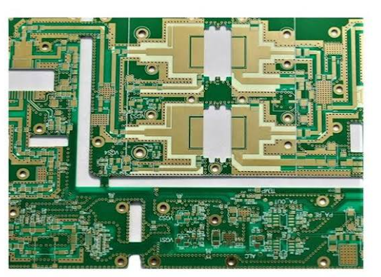
Multilayer Impedance PCB technology provides stable and predictable signal transmission for telecommunications, automotive electronics, industrial controls, computing, and other high-performance electronic systems. Unlike conventional PCBs, impedance-controlled multilayer boards require precise control of trace geometry, dielectric thickness, copper thickness, material properties, and stack-up configuration throughout the manufacturing process.
The manufacturing objective is not simply to produce a functional circuit board, but to maintain the specified impedance across the entire signal path. Small variations in materials or fabrication parameters can affect signal integrity, making engineering control and process consistency essential.
GOPCBA provides advanced PCB Manufacturing solutions covering multilayer, high-speed, high-frequency, HDI, controlled-impedance, and other complex PCB structures. PCB Manufacturing Services
1. Material Selection: The Foundation of Impedance Control
Materials form the foundation of Impedance PCB Manufacturing. The laminate system must be selected according to the target impedance, operating frequency, layer structure, thermal requirements, and application environment.
Dielectric Constant and Thickness
The dielectric constant (Dk) directly affects impedance characteristics. Materials with stable and predictable Dk values help maintain consistent impedance across different production lots and board areas.
For high-speed applications, low-loss materials may be selected to reduce transmission loss. Standard FR-4 materials can be suitable for many conventional applications when their electrical properties and manufacturing requirements are properly controlled.
Dielectric thickness is equally important. The distance between the signal trace and its reference plane directly influences impedance, so the selected core and prepreg thicknesses must match the approved stack-up.
Copper Thickness and Surface Roughness
Copper thickness must be considered together with trace width and dielectric geometry. Variations in finished copper thickness can change the effective trace geometry and therefore influence impedance.
Copper surface roughness is also increasingly important in high-frequency applications because rough copper surfaces can increase conductor loss. Material selection should therefore consider both copper thickness and surface characteristics.
For projects requiring complex material combinations and tight dimensional control, GOPCBA publishes detailed PCB Capabilities covering dielectric thickness, copper features, HDI structures, and other manufacturing parameters. PCB Capabilities
2. Core Manufacturing Processes for Precise Impedance Control
The production of a Controlled Impedance PCB requires coordinated control of the inner layers, lamination, drilling, plating, outer layers, and solder mask. Each process can influence the final electrical characteristics.
Inner-Layer Imaging and Etching
Inner-layer fabrication determines the geometry of many impedance-controlled traces. Trace width must remain within the engineering tolerance established during stack-up and impedance calculations.
Advanced imaging processes can provide precise circuit pattern transfer, while controlled etching helps minimize excessive side etching and dimensional variation.
Over-etching can reduce trace width and alter impedance, while insufficient etching can leave traces wider than specified. For this reason, etching parameters should be adjusted according to copper thickness, material construction, and circuit geometry.
After etching, automated optical inspection can identify open circuits, shorts, abnormal trace widths, and other defects before the inner layers proceed to lamination.
Lamination: Controlling Dielectric Thickness and Registration
Lamination is one of the most important stages in Multilayer PCB manufacturing because it determines the final relationship between signal layers, reference planes, and dielectric materials.
The approved stack-up defines the required combination of copper foils, cores, and prepreg. Prepreg selection and resin content must be matched to the required post-lamination dielectric thickness.
During lamination, temperature, pressure, resin flow, and cooling conditions must be controlled to achieve consistent dielectric thickness and minimize warpage.
Layer registration is equally important. Misalignment between signal layers and reference planes can affect both electrical performance and manufacturing reliability.
GOPCBA’s technical resources describe lamination as a critical process for multilayer and high-speed PCB structures, particularly where stack-up and impedance requirements must remain tightly controlled. High-Speed PCB Lamination Guide
Drilling and Copper Plating
Drilling creates the interconnections between PCB layers. Hole diameter, position accuracy, aspect ratio, and hole-wall quality all influence interconnection reliability.
After drilling, desmear and hole-wall preparation processes help ensure reliable copper deposition. Electroless copper and subsequent electroplating build the conductive structure inside the holes.
Copper thickness should be controlled consistently across the board. Uneven plating can change conductor geometry and introduce variations that affect impedance-controlled structures.
For advanced multilayer boards, blind vias, buried vias, and microvias may also be incorporated according to the design requirements.
Outer-Layer Etching and Solder Mask
Outer-layer etching follows principles similar to inner-layer fabrication, but external impedance traces must also account for the influence of the solder mask.
Trace width compensation may be incorporated during engineering preparation to account for manufacturing effects. Solder mask thickness and dielectric properties can influence the effective impedance of surface traces, particularly in high-speed designs.
Therefore, solder mask application must be controlled for thickness, coverage, registration, and curing consistency.
3. Impedance Testing and Final Inspection
Impedance testing is a critical part of Controlled Impedance PCB production because it verifies whether the finished board matches the specified electrical requirements.
Impedance Testing
Test coupons can be incorporated into the production panel to represent the electrical characteristics of the finished PCB. Depending on the project requirements, testing may use time-domain reflectometry (TDR) or other appropriate impedance measurement methods.
The measured impedance should be compared against the customer’s specified target and tolerance. Any deviation should trigger engineering investigation before the affected production lot is released.
GOPCBA’s high-speed PCB manufacturing information identifies impedance testing, including TDR coupon testing where required, as part of advanced PCB production and quality control. High-Speed PCB Manufacturing Guide
Visual and Dimensional Inspection
Final inspection should verify solder mask, silkscreen, surface finish, exposed copper, board dimensions, hole sizes, spacing, and other mechanical characteristics.
Electrical testing can additionally verify circuit continuity and isolation, helping identify manufacturing defects before shipment.
Reliability Testing and Traceability
Depending on the application, reliability testing may include cross-section analysis, solderability evaluation, adhesion testing, thermal testing, or other project-specific tests.
Production traceability is also important. Material information, process parameters, inspection results, and manufacturing records should be maintained so that quality issues can be investigated efficiently.
4. Full-Process Production Control for Custom Requirements
The key to consistent Impedance PCB Manufacturing is controlling materials, processes, and finished products as one integrated system.
Incoming Material Control
Incoming inspection should verify critical parameters such as:
- Laminate type
- Dielectric thickness
- Dk characteristics
- Copper thickness
- Prepreg specification
- Resin content
- Surface condition
- Solder mask material
Materials that do not meet the approved specification should not enter production.
Process Control
Critical manufacturing parameters should be monitored throughout imaging, etching, lamination, drilling, plating, solder mask application, and surface finishing.
Engineering records should connect process parameters with the corresponding production lot so that deviations can be identified and corrected quickly.
Finished Product Control
Finished boards should undergo appropriate electrical, dimensional, visual, and impedance testing before shipment.
GOPCBA’s quality management system describes control across PCB design review, DFM checking, PCB manufacturing, testing, incoming materials, and production processes, with electrical testing applied to manufactured PCBs. GOPCBA Quality Management
5. Flexible Manufacturing for Custom Multilayer Impedance PCBs
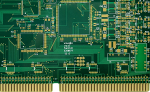
Customer requirements for Multilayer PCB products are increasingly diverse. Different projects may require different layer counts, materials, impedance targets, copper weights, board thicknesses, and signal frequencies.
A flexible manufacturing system must therefore support rapid changes between different board configurations while maintaining process stability.
Engineering teams should evaluate customer specifications before production, including:
- Layer count
- Stack-up
- Material system
- Controlled impedance values
- Trace width and spacing
- Copper thickness
- Finished board thickness
- Via structures
- Surface finish
- Electrical testing requirements
DFM analysis can identify manufacturing risks before fabrication begins and provide opportunities to optimize the design for production.
For high-density applications, HDI structures can further increase routing capability through microvias, blind vias, buried vias, and sequential buildup technology.
6. Future Trends in Multilayer Impedance PCB Manufacturing
As electronic systems move toward higher data rates and greater circuit density, the requirements for High-Speed PCB manufacturing continue to increase.
Impedance tolerances may become tighter, while low-loss materials, more advanced stack-ups, finer circuit geometries, and more sophisticated testing methods become increasingly important.
At the same time, customers increasingly require smaller production volumes, more product variations, and shorter development cycles. PCB manufacturers therefore need both high-precision fabrication and flexible production capabilities.
Advanced manufacturing technologies such as laser direct imaging, HDI, microvias, low-loss laminates, precision lamination, and controlled copper plating will continue to play an important role in supporting next-generation electronic systems.
Conclusion
Custom Multilayer Impedance PCB manufacturing is a comprehensive engineering process rather than a single fabrication operation. Material selection, Dk and dielectric thickness, copper geometry, stack-up design, etching, lamination, drilling, plating, solder mask, and impedance testing must work together to achieve predictable electrical performance.
By combining precise process control with engineering review, DFM analysis, advanced multilayer fabrication, and comprehensive inspection, GOPCBA provides reliable solutions for communication, automotive, industrial control, computing, and other high-speed electronic applications.