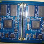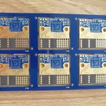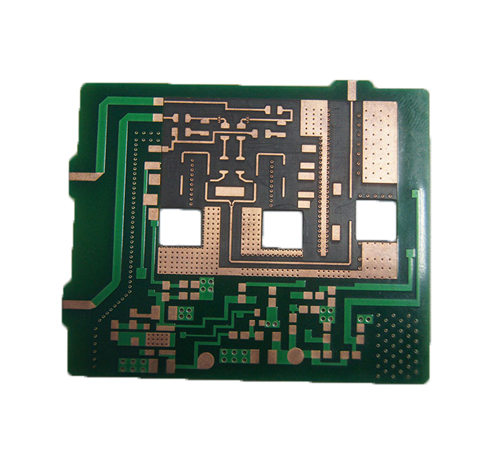
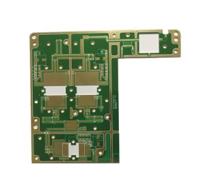
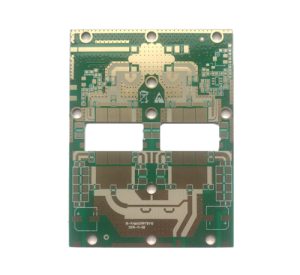
A high-frequency PCB is generally designed for applications in which signal frequencies extend into the high-hundreds-of-megahertz, gigahertz, or even millimeter-wave range. These boards are widely used in automotive radar, satellite communications, wireless communication equipment, RF systems, high-speed networking, and other advanced electronic applications.
As signal frequencies and edge rates increase, PCB routing becomes much more than simply connecting components. Trace geometry, dielectric properties, reference planes, vias, impedance, return-current paths, and the spacing between neighboring signals can all affect system performance.
For this reason, high-frequency PCB routing must be designed with transmission-line behavior and signal integrity in mind. Poor routing can cause signal reflection, crosstalk, electromagnetic interference (EMI), excessive ringing, timing errors, and even communication failures.
This guide explains the fundamental principles and practical routing rules for designing reliable high-speed PCB systems.
When Does PCB Routing Become a High-Frequency Problem?
At relatively low frequencies, many PCB interconnections can be treated approximately as lumped circuits. As signal frequency increases, however, the electrical length of a trace becomes significant compared with the signal wavelength.
A simplified relationship is:
λ = v / f
where:
- λ is the signal wavelength
- v is the propagation velocity
- f is the signal frequency
The propagation velocity is affected by the PCB dielectric material and transmission-line structure, so it is normally lower than the speed of light in air.
More importantly, frequency alone does not determine whether transmission-line effects matter. A digital signal with a very fast rise time can exhibit transmission-line behavior even when its clock frequency appears relatively low.
Therefore, modern high-speed PCB design should consider both operating frequency and signal rise/fall time.
Why Impedance Matching Matters in High-Frequency PCB Routing
When a high-speed signal travels through a PCB transmission line and encounters an impedance discontinuity, part of the signal can be reflected toward the source.
The basic principle is:
Reflection coefficient Γ = (ZL − Z0) / (ZL + Z0)
where:
- ZL is the load impedance
- Z0 is the characteristic impedance of the transmission line
When the load impedance is close to the characteristic impedance, signal reflection is reduced.
This is why impedance matching is essential for high-speed interfaces and RF circuits.
The characteristic impedance of a PCB transmission line is influenced by:
- Trace width
- Copper thickness
- Dielectric thickness
- Dielectric constant (Dk)
- Distance to the reference plane
- Trace geometry
- Copper roughness
- Solder mask
- Differential-pair spacing
For example, many differential interfaces use a nominal differential impedance of 90 Ω, 100 Ω, or another application-specific value. The exact target must always follow the interface specification and system design requirements rather than relying on a universal trace-width rule.
Key High-Frequency PCB Routing Rules
Effective high-frequency PCB routing requires careful control of routing length, layer transitions, spacing, reference planes, and return-current paths.
1. Minimize Unnecessary Vias
Every via introduces a discontinuity into the transmission path. Depending on its geometry and surrounding structure, a via can introduce parasitic capacitance and inductance.
Too many vias can therefore increase insertion loss, impedance discontinuity, and signal distortion.
For critical high-speed signals:
- Minimize unnecessary layer changes.
- Keep via structures consistent.
- Avoid unnecessary via stubs.
- Use appropriate back-drilling or HDI structures when required.
- Maintain a continuous reference plane around critical signal transitions.
The objective is not simply to eliminate every via, but to use vias only when they provide a necessary routing or interconnection function.
2. Keep High-Speed Traces Short and Direct
Shorter traces generally reduce propagation delay, attenuation, radiation, and opportunities for unwanted coupling.
Critical signals such as:
- Clock signals
- LVDS
- DDR data and clock
- USB
- HDMI
- PCIe
- RF signals
should generally use short, direct routing with as few discontinuities as practical.
Avoid unnecessary branches and stubs, particularly on very high-speed interfaces.
3. Avoid Sharp Routing Changes
Sudden changes in trace geometry can create impedance discontinuities.
Instead of unnecessary 90-degree corners, use 45-degree routing or smooth curved transitions where appropriate.
For RF and microwave structures, routing geometry should be even more carefully controlled because small dimensional changes can affect impedance and phase characteristics.
How to Reduce PCB Crosstalk
PCB crosstalk is unwanted coupling between adjacent signal structures. It is caused primarily by electromagnetic coupling between traces and can become more significant when signals have fast edges, long parallel sections, or insufficient spacing.
Crosstalk can be divided broadly into capacitive and inductive coupling. Both are affected by trace spacing, parallel routing length, signal transition speed, stack-up, reference-plane configuration, and driver characteristics.
The following techniques can significantly improve crosstalk control.
1. Increase the Spacing Between Critical Signals
Increasing the distance between adjacent signal traces reduces electromagnetic coupling.
When board space permits:
- Increase spacing between critical traces.
- Reduce the length over which traces run in parallel.
- Separate sensitive analog signals from noisy digital signals.
- Keep high-speed clocks away from low-level analog circuits.
The appropriate spacing should be determined from the stack-up and impedance requirements rather than applying one fixed spacing rule to every PCB.
2. Use a Continuous Ground Reference
A continuous reference plane provides a low-inductance return-current path and helps contain electromagnetic fields around transmission lines.
For high-speed signals, avoid routing across:
- Ground-plane splits
- Power-plane gaps
- Large voids
- Slots
- Unintended plane discontinuities
A signal trace may appear electrically connected from the source to the receiver while its return path is interrupted. This can increase loop area and cause EMI and signal-integrity problems.
3. Reduce Parallel Routing Length
If two high-speed traces must run near each other, minimizing their parallel length can reduce coupling.
This is especially important for:
- Clock and data signals
- High-speed differential pairs
- RF and digital signals
- Sensitive analog and switching-node signals
A practical routing strategy is to separate critical traces as soon as possible rather than allowing them to run in parallel for long distances.
4. Avoid Excessive Parallel Routing on Adjacent Layers
When two signal layers are used for high-speed routing, their routing directions can be arranged orthogonally where practical.
For example, if one signal layer predominantly routes horizontally, an adjacent signal layer can favor vertical routing.
However, the most important consideration remains the reference-plane structure and actual electromagnetic coupling. Orthogonal routing is a useful strategy, but it should not replace proper stack-up and spacing analysis.
Differential Pair Routing
Differential pair routing is widely used in high-speed communication interfaces because differential signaling can provide good common-mode noise rejection when properly implemented.
Typical examples include:
- LVDS
- USB
- HDMI
- PCIe
- Ethernet
- High-speed ADC/DAC interfaces
Important differential-pair routing considerations include:
Maintain Consistent Geometry
The two traces should maintain controlled:
- Trace width
- Trace spacing
- Reference-plane distance
- Copper thickness
- Dielectric environment
Abrupt changes in spacing or geometry can affect differential impedance and skew.
Match the Pair Length Where Required
The two traces should be length matched according to the interface timing requirements.
However, excessive serpentine routing should be avoided. Long meanders can introduce additional coupling and discontinuities.
Length matching should therefore satisfy the actual timing budget rather than simply making every trace exactly the same length.
Keep the Reference Plane Continuous
Differential routing still requires a controlled return-current path.
Do not assume that differential signaling completely eliminates the need for a good reference plane.
High-Frequency PCB Grounding Principles
PCB grounding is one of the most important factors in high-speed and RF design.
A good ground system provides:
- A low-impedance return path
- Reduced loop area
- Better EMI performance
- Improved signal integrity
- More stable reference potential
- Better isolation between circuit sections
Separate Sensitive Circuit Functions Appropriately
Analog, digital, power, and RF sections should be arranged according to their noise characteristics.
However, simply splitting the ground plane into multiple isolated regions is not always the best solution.
An improperly designed ground split can force return currents to take long paths around the split, increasing loop area and EMI.
A better approach is to control circuit placement, current paths, reference planes, and grounding connections as part of the overall PCB stack-up.
Use Ground Vias Strategically
Ground vias can provide low-inductance connections between ground layers and help establish controlled return-current paths.
For RF and high-speed structures, ground-via placement should be carefully coordinated with signal vias and transmission-line geometry.
Via fences may also be used in some RF applications to improve isolation and control electromagnetic fields.
Grounding High-Frequency Digital and Analog Circuits
High-frequency digital circuits generate substantial harmonic content because of their rapid transitions.
If digital return currents are allowed to flow through sensitive analog regions, unwanted coupling may occur.
Instead of automatically isolating digital and analog grounds, designers should first understand the current paths and system architecture.
Depending on the application, appropriate techniques may include:
- Controlled partitioning of analog and digital circuits
- Dedicated reference planes
- Strategic single-point connections
- Ground stitching vias
- Ferrite components where electrically justified
- Careful power-distribution design
The correct solution depends on the complete system rather than a single universal grounding rule.
High-Frequency Decoupling Capacitors
Every high-speed IC requires a stable power-delivery network.
High-frequency decoupling capacitors should be placed close to the relevant power pins to reduce the impedance between the IC and its local energy source.
Effective decoupling design should consider:
- Capacitor placement
- Via inductance
- Power and ground-plane geometry
- Capacitor package size
- Target frequency range
- Power-distribution impedance
A capacitor placed physically far away from the IC may provide much less effective high-frequency decoupling because the connecting traces and vias introduce parasitic inductance.
Therefore, placement is often just as important as capacitance value.
Practical Routing Guidelines for Common High-Speed Interfaces
LVDS Routing
LVDS generally uses controlled-impedance differential pairs.
Key considerations include:
- Follow the interface’s specified differential impedance.
- Keep the pair closely coupled and geometrically consistent.
- Minimize skew.
- Avoid unnecessary vias.
- Maintain a continuous reference plane.
- Place termination according to the transceiver specification.
A commonly used differential impedance target is 100 Ω, but the exact requirement should be confirmed from the specific LVDS device and interface design.
USB Routing
USB differential pairs require controlled impedance and careful routing.
Important considerations include:
- Maintain consistent differential-pair geometry.
- Keep the pair short where practical.
- Minimize stubs.
- Avoid unnecessary layer transitions.
- Keep the pair away from noisy switching nodes.
- Maintain a continuous reference plane.
- Follow the applicable USB specification and device manufacturer’s layout requirements.
A fixed value such as 10 mil trace width should not be treated as a universal USB routing rule because the required geometry depends on PCB stack-up and dielectric construction.
HDMI Routing
HDMI uses high-speed differential signaling, so controlled impedance and pair matching are critical.
Recommended practices include:
- Route each differential pair as a controlled-impedance structure.
- Keep the pair geometry consistent.
- Minimize vias and stubs.
- Match the differential-pair lengths within the required tolerance.
- Avoid unnecessary parallel coupling with other high-speed signals.
- Keep the reference plane continuous.
The exact trace width and spacing must be calculated from the PCB stack-up rather than copied as fixed values from another design.
DDR Routing
DDR interfaces are highly sensitive to timing, skew, impedance, and signal integrity.
Routing requirements depend strongly on the DDR generation and memory architecture.
Important considerations include:
- Match critical signal groups according to the memory interface timing budget.
- Control trace impedance.
- Minimize unnecessary vias.
- Maintain consistent reference planes.
- Avoid excessive stubs.
- Control address, command, clock, and data-group routing.
- Follow the memory controller and DRAM manufacturer’s layout guidelines.
The commonly referenced 2W spacing rule can help reduce coupling, but it should be treated as a design guideline rather than a universal DDR requirement.
High-Frequency PCB Stack-Up Considerations
Routing quality is closely related to PCB stack-up design.
A suitable stack-up should provide:
- Stable reference planes
- Controlled dielectric thickness
- Appropriate signal-layer arrangement
- Controlled impedance
- Short return-current paths
- Adequate power-distribution performance
For high-speed multilayer boards, stripline and microstrip structures are commonly used depending on the required impedance and electromagnetic environment.
For RF applications, the stack-up may also need to account for dielectric loss, copper roughness, surface finish, and material anisotropy.
Common High-Frequency PCB Routing Problems
Several routing mistakes can significantly degrade signal integrity.
Routing Across a Plane Split
This can interrupt the return-current path and increase electromagnetic radiation.
Excessive Via Stubs
Long unused portions of vias can behave as unwanted transmission-line structures and cause resonances or reflections.
Long Parallel Traces
Long parallel routing between aggressive and sensitive signals increases crosstalk.
Inconsistent Differential-Pair Geometry
Changes in width or spacing can cause impedance variation and differential skew.
Poor Decoupling Placement
A theoretically correct capacitor may provide limited high-frequency performance if it is connected through long traces or high-inductance vias.
Excessive Length Matching
Unnecessary serpentine routing can increase coupling and should not be used simply to make every trace visually identical.
How Kingda Supports High-Frequency PCB Manufacturing
High-quality high-frequency PCB production requires close coordination between PCB design and manufacturing.
Kingda can support high-speed and RF PCB projects by focusing on:
- Controlled PCB stack-up
- High-frequency material selection
- Trace width and spacing control
- Impedance-controlled fabrication
- Layer registration
- Drilling and via accuracy
- Copper thickness control
- Surface-finish consistency
- Electrical testing
- Manufacturing inspection
For complex high-speed boards, design-for-manufacturing (DFM) analysis should be performed before production to identify potential issues involving impedance, minimum spacing, via structures, registration, and material selection.
Conclusion
Successful high-frequency PCB routing requires much more than simply connecting components. As signal rise times become faster and operating frequencies increase, PCB traces behave increasingly like transmission lines.
Designers must therefore control impedance matching, return-current paths, trace geometry, differential-pair routing, grounding, via structures, and PCB crosstalk.
The most important principles are to keep critical signals short and direct, minimize unnecessary vias and stubs, maintain continuous reference planes, control differential-pair geometry, reduce long parallel routing, and design the PCB stack-up together with the routing strategy.
By combining careful PCB design with controlled manufacturing processes, engineers can achieve better PCB signal integrity, lower EMI, and more reliable performance in high-speed communication, automotive, RF, aerospace, and other advanced electronic applications.