




Half-Bridge Converter Layout: Power, Gate Drive and Ground
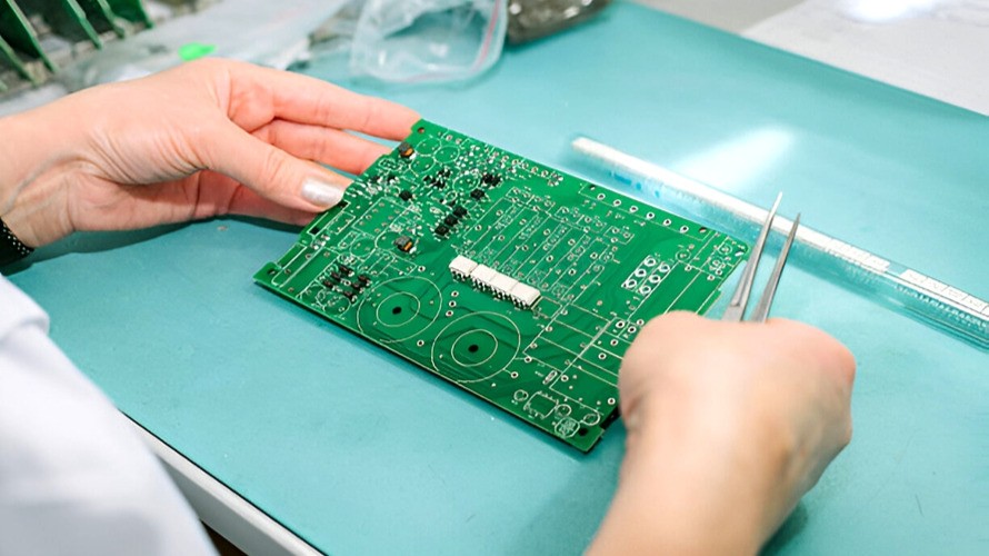
A half-bridge converter is a switching power stage, and its layout decides whether the efficiency calculated on paper survives contact with the board. The currents are large, the edges are fast, and the same node that carries the main power also carries the switching noise that will be coupled into every sensitive circuit nearby if the geometry allows it. The material below covers the sequence that matters: where the parts go, how the high-current and gate paths are routed, how the grounds are arranged, how heat is removed and how emissions are contained.
Placement
Placement settles most of the layout before a single trace is drawn.
The power MOSFET devices belong where their heat can leave. In practice that means near a board edge or in a position where a heatsink can be fitted and where the thermal path to the enclosure is short. The two devices in the bridge should be placed so that the high-current loop between them, the transformer and the input capacitance is as small as the mechanical constraints allow, and so that they are not coupled into each other magnetically more than the topology requires.
The transformer sits centrally, in a region shielded by the surrounding copper and away from sensitive analogue traces. Its location also determines the length of the primary and secondary connections, and those lengths are part of the loss and the radiated field, so the placement should be chosen to keep both short rather than to make the layout tidy.
The control device belongs in a quiet area, away from the switching node and away from the high-current path. Its support components — the feedback network, the compensation components, the timing element — should surround it closely, because each of them is a sensitive node and the shorter their connections are, the less they pick up.
The input capacitors belong at the switching devices, not at the input connector. Their purpose is to supply the current the bridge draws in short pulses, and the loop they form with the devices is the smallest loop in the design and the most important one to minimise. Placing them further away enlarges that loop and converts the capacitor into a filter that is too far from the noise to help. The output capacitors follow the same logic, placed close to the load side of the rectifier.
Routing the High-Current Paths
The high-current path includes the device source-to-drain loop, the transformer windings and the connections between them. These traces carry both the average current and the switching current, and their inductance is what turns a fast edge into a voltage spike and a radiating loop.
Two rules follow. The first is width: the conductors should be as wide as the layout reasonably allows, sized from the current and the acceptable temperature rise rather than from habit. The second is shape: the path should be direct, without sharp changes of direction and without branches, because both are local changes in impedance that reflect part of the switching energy back into the circuit.
The most useful structural decision is to make the loop physically small. A power stage with a compact loop radiates less, rings less and is easier to filter, and the payoff is larger than any improvement in the components.
Gate Drive Routing
The gate circuit is a loop built around the device capacitance, and it carries a fast current pulse that both radiates and can be disturbed by its surroundings.
The trace from the driver to the gate should be short and reasonably wide, because its inductance opposes the current that has to flow to charge the gate and slows the switching transition. A long thin gate trace produces slow switching and, with it, additional switching loss in the device.
The return path matters as much as the outgoing one. The gate current returns through the source connection, so the source trace has to be part of the design intent rather than a convenient connection to the ground plane. Running the gate trace and its return close together keeps the loop small and reduces the field the pair produces.
Separation from the high-current path is the other requirement. A gate trace routed alongside a switching node picks up the displacement current from that node and can be driven into unintended conduction. Where the two must cross, crossing is preferable to running in parallel, and where they must run near each other, a ground trace between them is worth the space.
A buffer or gate resistor placed close to the device is often worth including. It damps the ringing that the gate loop would otherwise produce and gives the designer a way to trade switching speed against noise without changing the layout.
Grounding
Power converters are where ground design turns from an abstract rule into a measurable effect.
The usual arrangement separates the grounds by function: the power ground that carries the switching current, the signal ground that references the control circuit, and any analogue ground the design may have. Each is routed as its own network and joined at a defined point, so that the large currents flowing in the power ground do not develop a voltage across the path the sensitive circuits use as a reference.
This single-point grounding makes the reference unambiguous. Spreading the connections across the board makes the two networks share paths, and the resulting potential difference between them appears in the measurement and control circuits as noise that no amount of filtering will remove.
The ground conductors themselves should be wider than the signal traces, with the width following the current they carry, and they should follow the paths they serve. A ground connection that takes a long route to reach a via introduces impedance into the return path at exactly the point where the current is changing fastest, which is the least forgiving place to put it.
Thermal Path
Removing heat from the switching devices is a layout function as much as a mechanical one.
The first element is a copper area under each device, large enough to spread heat into the board, connected through a cluster of plated vias to copper on the other side or to an internal layer. The vias should be numerous and plated through the full thickness, since a thermal path is only as good as its narrowest point.
The second element is separation. Sensitive components should not be placed in the region where the heat from the switches spreads, because their behaviour changes with temperature: a capacitor loses life at elevated temperature, and a reference or a timing component drifts. Leaving space around the power devices and avoiding placing small parts directly beside them is a design decision with a measurable effect on reliability.
Where the board alone cannot remove the heat, a heatsink is part of the design rather than an accessory. Its mounting position, the surface finish beneath it and the interface material between it and the device all have to be planned while the layout is open, since the space it occupies cannot be recovered later.
Emissions and Filtering
A switching converter is a noise source by construction, and the design objective is to keep the noise local.
Containment starts with the loop areas already discussed and continues with the arrangement of the input and output filters. The input filter belongs as close to the stage as the input capacitor, and its components should be arranged so that the filter itself does not create a new loop that radiates. Because a filter and a converter can interact, the filter also has to be stable with the impedance the converter presents; a filter designed for attenuation alone can make the converter oscillate.
Where the design has a metal enclosure or a shielded area, the board layout should be arranged so that the printed copper, the enclosure and the mounting points together form a continuous shield around the noisiest region. The shield works only if it is bonded at short intervals; a single connection point leaves it as an antenna.
Verification
Three measurements answer most of the questions a layout raises.
The switching node waveform shows the ringing that the loop inductance produces and the effectiveness of any snubber or gate damping. The temperature of the switching devices at full load and at the worst supply condition shows whether the thermal path is adequate. And the conducted and radiated emissions measurements in the qualification test show whether the filtering and shielding decisions were sufficient — and the point at which failures appear often identifies the loop or the path responsible.
Because these measurements come late, the design decisions that make them likely to pass have to be taken early. The relevant general principles, including how a return path is established and how a loop’s area affects what it radiates, are the same ones described in the note on power and ground in mixed-signal layout, and the arrangement of the supply network that feeds a high-current load is covered in the guide to power delivery system design. The related selection of copper weight for the conductors that carry the current is discussed in the article on heavy copper in HDI boards.
FAQ
Why must the input capacitor be next to the switching devices? Because the loop it forms with them carries the pulsed switching current. Every millimetre of distance enlarges that loop, and the loop is what radiates and rings.
Why separate power and signal grounds? So that the voltage developed by switching current in the power ground does not appear in the reference the control circuit measures against. The two are joined at one point to keep the reference defined.
How wide should the gate trace be? Wide enough that its inductance does not slow the gate current significantly, and short for the same reason. The gate loop, not just the gate trace, is what has to be kept small.



2 Comments
Automotive Power MOSFETs
[…] The geometry of that arrangement, and the loop areas it creates, are the same ones examined in this note on half-bridge converter layout. […]
Motor Driver PCB Design: Layout and Thermal Rules - Kingda
[…] The geometry of a bridge arm is where this is decided, and the reasoning is the same as that described in this note on half-bridge converter layout. […]