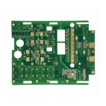
AI Server PCB Design: HDI, High-Speed Buses and Power
The boards inside a training cluster are no longer oversized server motherboards. They are high-layer-count interconnect carriers whose job is to move hundreds of gigabytes per second between accelerators and to deliver several hundred watts to each of them without sagging. An AI server PCB design has to satisfy three constraints at once: a very dense escape from large packages, a channel loss budget that survives long traces, and a power and thermal design that keeps every rail inside specification while the rack runs flat out.
What Separates a Server Board From a Workstation Board
A workstation board serves one processor and a handful of memory channels. A server board of the same generation may carry two sockets, eight or more accelerators, dozens of DIMM slots and a switching fabric between them, all inside a fixed rack unit. The electrical consequences are straightforward: the average trace is much longer, the average current is much higher, and the number of nets that must be length-matched grows from a few hundred to several thousand.
The mechanical consequences matter just as much. A large board with heavy copper and big heatsink mounting hardware will sag during reflow if the panel is not supported properly, and a board that warps after assembly will crack solder joints on the largest packages first.
HDI Technology and the Escape Problem
The largest packages on these boards present more than a thousand balls on a pitch that a through-via cannot escape. HDI technology solves it by adding laser-drilled microvias in a build-up pair on the outer layers, so that a ball grid can be fanned out in two or three short hops before the routing drops into the conventional core. Typical geometry is a 0.1 mm microvia in a 0.25 mm pad with a 0.15 mm annular ring, and two microvias stacked at most unless the fabricator qualifies more.
Count the layers from the escape, not from the netlist. If the accelerator package needs eight layers to get out and the memory bus needs six more, the board is a 20-plus layer design before any plane is added. Trying to squeeze that into fewer layers produces routing that is electrically fine on paper and impossible to fabricate.
High-Speed Signal Transmission Across Long Channels
high-speed signal transmission on a server board is a channel design problem. A link between two accelerators may cross 300 mm of board and two connectors, and at 32 Gbps every millimetre of loss and every impedance discontinuity takes a share of the eye diagram. Route differential pairs with a controlled impedance of 85 to 100 ohm, keep them on one layer as far as the floorplan allows, and use back-drilled or blind vias to remove the stub that would otherwise resonate in the band of interest.
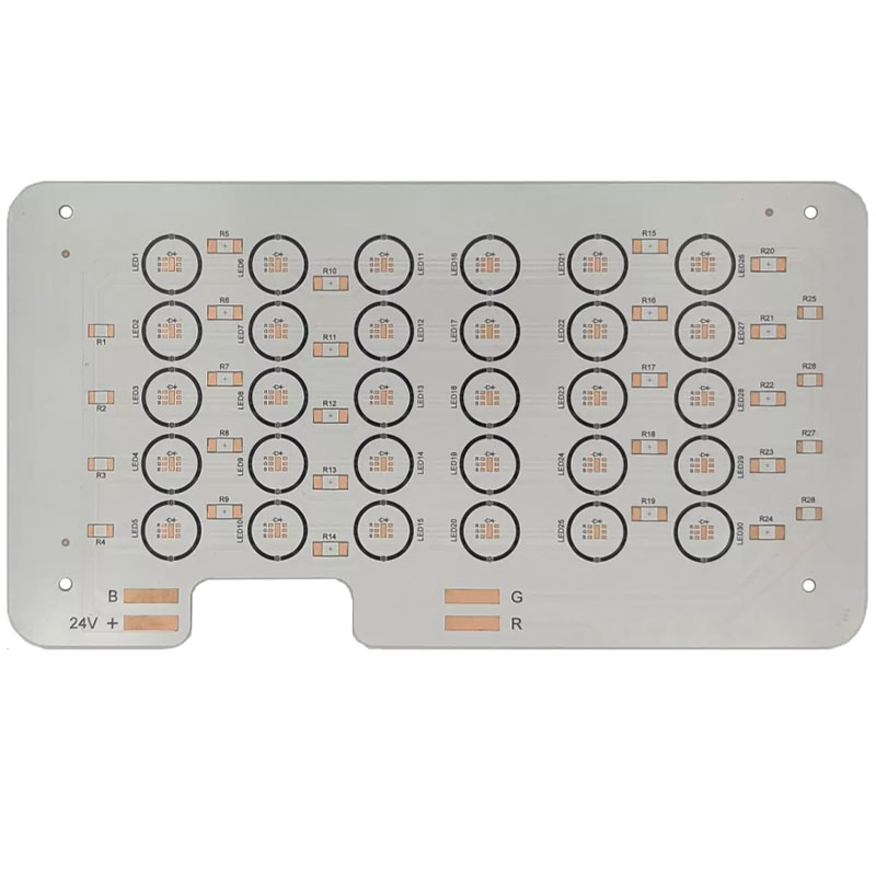
High frequency traces and data bus routing rules become mandatory rather than advisory here: no layer changes without ground stitching, no plane splits under a link, and no long parallel runs between a link and a switching supply. Skew within a pair should stay under 0.15 mm, and skew between lanes in the same group under 2 mm.
Power Distribution Network and Copper Weight
The power distribution network on a server board delivers several hundred amperes at less than one volt. That current is carried by copper planes, and resistance, not inductance, is usually the limiting factor: a milliohm of plane resistance at 400 A is 0.4 V of drop, which is more than the whole regulation window. Use trace width and current calculation to size the necks, then double the answer for the plane areas where the current converges under a socket.

Heavy copper helps but has limits. Two ounces of copper on an inner layer is common; beyond that, etching fine features becomes difficult and the fabricator will push back. It is usually better to add a dedicated power layer pair and split it into voltage islands than to push copper weight further. Decoupling goes on the underside of the socket, as close to the power balls as the layout allows, and the loop from the capacitor to the via pair to the plane should be as short as it can physically be made.
Thermal Management and Material Choice
thermal management starts with the stackup. A board carrying 400 W of accelerator load and 200 W of memory has to move that heat somewhere, and the paths are the copper, the thermal vias under each package, and the mechanical attachment to the chassis. Fill and cap the thermal via arrays so they can also carry current and so that solder does not wick away during assembly.
Material choice follows the loss budget. Standard FR-4 with a high glass transition temperature is adequate for the lower-loss links, but the longest channels usually need a mid-loss or low-loss laminate, and very long backplane links need a low-loss material with a stable dielectric constant across temperature. Mixing materials in one stackup is normal and cost-effective, as long as the fabricator can bond them without delamination. Layer stackup planning principles apply at every scale: keep the signal layers symmetric about the centre, keep the dielectric thicknesses balanced, and place the reference planes so that no signal layer is more than one dielectric away from a solid return.
Fabrication Class and Tolerances to Agree Early
Agree the fabrication class before layout starts. Fine lines below 3 mil, laser microvias, back-drilling, heavy copper and impedance control within 5 percent are all available, but not from every supplier and not at every layer count. Impedance coupons should be placed on the panel so that the measured value can be traced back to a specific stackup, and the drill schedule should be reviewed before the first panel is released.
Panels also dictate yield. Boards this large rarely fit many per panel, so small changes in outline size can shift the whole cost structure. Check the fabricator’s maximum panel size and the rail requirements before fixing the outline.
Test, Inspection and Reliability
Flying probe or fixture test has to reach every net, which is difficult on a board full of fine-pitch packages. Plan test points for the rails, the reset lines and the management bus, and accept that some nets will only be verified through boundary scan. For long-life installations, add a thermal cycling qualification on the assembled board rather than on coupons alone, because the failure modes that matter here are at the package-to-board interface.
FAQ
How many layers does an AI server board need? Most current accelerator carrier boards run from 16 to 24 layers, with the count set by the escape from the largest package plus the memory and fabric buses. Start from the fanout and let the plane count follow.
Is HDI always necessary? No. If the largest package can escape with through vias and the link lengths are short enough, a conventional multilayer stack is cheaper and easier to fabricate. HDI earns its cost when ball pitch, ball count or routing density makes a through-via escape impossible.
How should the loss budget be divided between material and geometry? Measure the channel first. If a low-loss laminate removes enough loss to keep the link inside its specified eye mask without equalisation, it is usually cheaper than adding layers or retimers. If it does not, fix the geometry before spending on material.