Via Plugging Process Control for PCB Assembly
A via is drilled and plated to connect layers, but on a finished board it is also a hole in the surface that solder, flux and cleaning chemistry can enter. The via plugging process exists to close that hole in a controlled way, so the surface behaves as if the via were never there. Getting it right means choosing a class of plug, matching it to the surface finish, and controlling ink viscosity and cure.
Why Vias Get Plugged
An open via causes three practical problems. Solder can wick through the barrel during wave soldering and appear on the component side as a bead or a short. Flux and cleaning residue can be trapped inside the barrel and leak out later as contamination under a conformal coating. And in a fine-pitch array, a via that sits on or beside a pad can draw paste away from the joint, which is a defect that only appears after reflow.
The usual response is to define acceptance classes rather than a single specification, because the right answer depends on what the via has to do afterwards.
The Three Acceptance Classes
The first class is a via that only has to be covered: solder mask is bridged across the opening and nothing else changes. The second requires the barrel to be filled and the surface flat enough to place a pad over it, typically within 25 micrometres of the surrounding surface. The third requires a fully filled, plated and planarised via that forms part of the electrical pad itself. Cost rises steeply with the class, so the fabrication drawing should name the class for each via group instead of applying one rule to the whole board.
Two questions usually settle the argument. If the via sits on a pad it must be filled and capped, because an open barrel under a paste deposit pulls solder away from the joint. If the via merely sits beside a pad, tenting is normally enough.
Tenting Versus Full Plugging
tenting is the cheapest option: the mask is printed so that it spans the via opening and the ink cures across it. It is adequate when the via is not on a pad and the board will not see a second wave-solder pass. It fails when the opening is large, because the ink sags into the barrel and leaves a dimple that survives curing, and it becomes unreliable once the opening exceeds roughly 0.5 mm.
Full plugging fills the barrel with a dedicated ink and levels it. This is the process used for via in pad and for any via that has to survive thermal cycling without pumping. Where a pad sits on the via, the fill should be capped with copper, which means plating after filling, and that in turn means the plating line has to handle an already cured organic surface. Electroplating and via filling in HDI covers the copper side of that sequence.
Via in Pad and Fine-Pitch Escapes
via in pad removes the escape routing a conventional fanout would need, and it is often the only way to fit a dense ball array under a package. The trade is that the via becomes part of the joint: any void, any dimple, or any ink that is not fully cured will appear as a void in the solder or as outgassing during reflow. Vias in pad need filled and capped construction, flatness of about 25 micrometres, and a copper cap thick enough to survive plating and planarising. Via in pad or plated through is the cost decision that precedes this process choice.
Plugging Before or After Surface Finish
The sequence matters as much as the chemistry. Plugging before the surface finish lets the ink cure through a full thermal cycle, which gives better dimensional stability and avoids the mask lifting that happens when a cured ink meets hot air levelling. It does mean the finish is applied over cured organic material, so the finish chemistry must not attack it.
Plugging after hot air levelling is simpler for the fabricator and common on boards with many vias to close. Its weakness is thermal shock: the panel is already hot when the ink goes in, and the cure that follows can pull the ink away from the barrel wall. Whichever order is used, keep the plugging ink and the solder mask in the same chemistry family, because the interface between them is where defects start.
Ink Selection, Viscosity and Curing
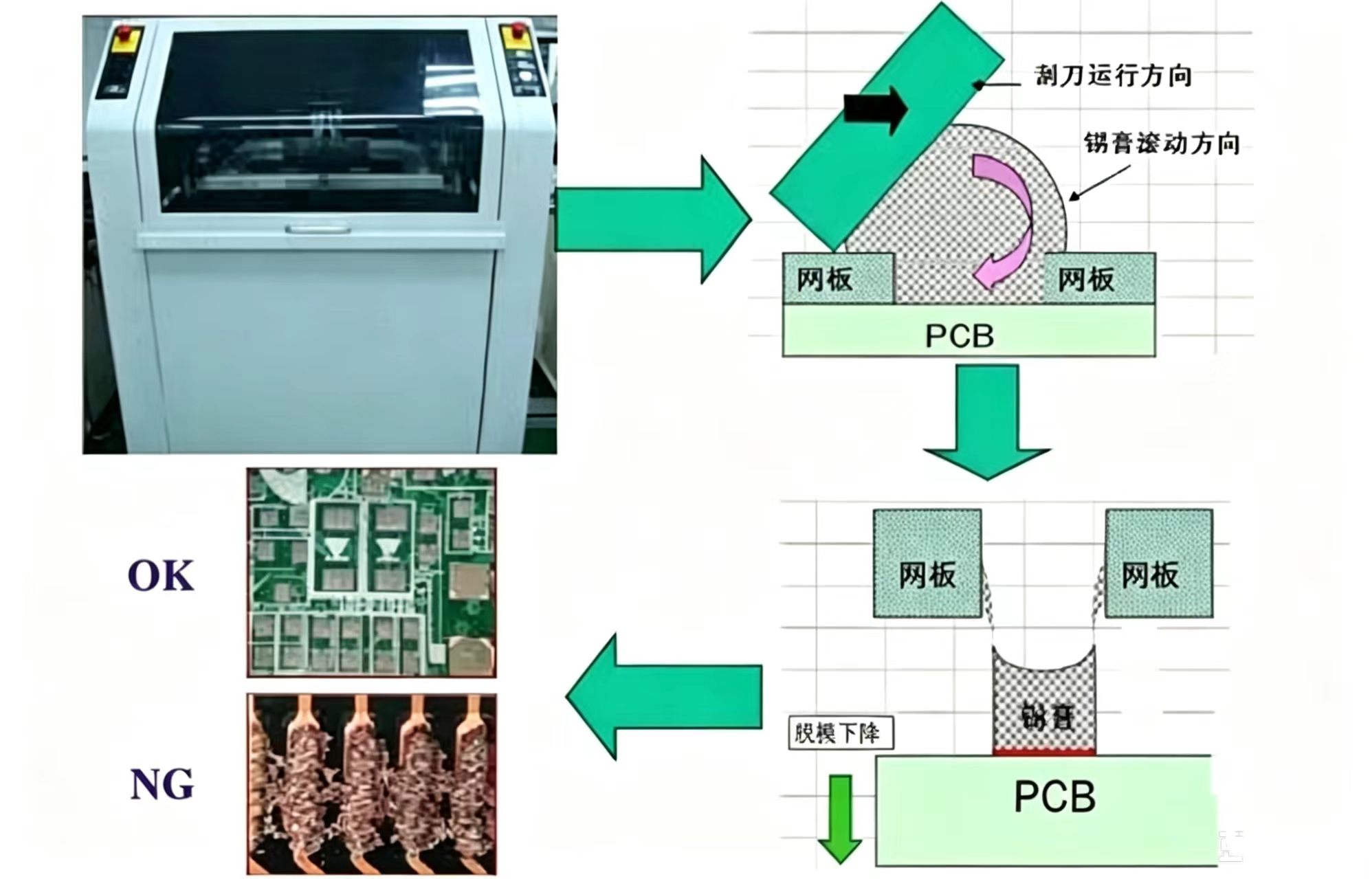
Plugging ink is chosen for solids content and shrinkage, not only for colour. A high-solids thermal-cure ink that shrinks less than two percent will fill a barrel in one pass and stay put. A low-viscosity ink slumps during storage and leaves a dimple at the top of the hole. Thixotropy, the way the ink behaves under shear, decides whether it stays on the stencil or bleeds beneath it; solder mask ink thixotropy explains the measurement behind those printer settings.
curing has to be complete and uniform. A two-stage profile, a lower temperature to drive off solvent followed by a full cure at the specified temperature, gives a better result than one long bake. Under-cured ink outgasses in the reflow oven and blows a bubble through the mask. Over-cured ink turns brittle and cracks at the via edge during thermal cycling, which is a defect that only shows up in the field.
Defects, Causes and Fixes
Voids come from air trapped in the barrel or solvent that cannot escape, and they are the most common reason a first article fails microsection. Bleed is ink that flows onto the surrounding pad and reduces the solderable area; it usually follows excessive print pressure or too low an ink viscosity. Mask lift at the via edge is nearly always a cure or a cleaning problem rather than a printing problem. Solder wicking into a via during assembly points back to the tenting decision, because that via should not have been left open.
Since the acceptance criteria are dimensional, the inspection method has to be dimensional as well. One cross-section per panel is the usual check, with hole fill percentage and cap thickness measured, plus a visual scan for dimples and for ink on pads.
Keeping the Process Under Control
Plugging is a wet process, so the variables that matter drift with time and temperature. Record the ink batch, the print pressure, the squeegee speed, the snap-off distance and the cure profile for every panel, and re-measure the ink viscosity at the start of each shift. When a defect appears, the record is what tells you whether the ink changed or the machine did. Panels should also be allowed to cool before handling, because a warm plugged via is soft enough to mark, and handling damage at this stage looks exactly like a filling defect.
FAQ
Does every via need to be plugged? No. Vias that are covered by mask, away from pads and not exposed to a second soldering pass can stay open. Plug only what the assembly process requires, because each plugged via adds process steps and inspection.
How flat does a filled via have to be? For a via that will carry a solder joint, flatness within about 25 micrometres of the surrounding surface is a common requirement. A dimple deeper than that will trap flux or leave a void under the paste.
Can plugged vias be reworked? Rarely. Once the barrel is filled and cured, the ink cannot be removed selectively without damaging the surrounding mask. Treat the plugging step as irreversible and inspect before the panel moves on.