Key Production Processes for High Layer Count PCBs
Average layer count has become one of the standard measures of a board shop’s technical level, and for good reason. High layer count PCBs are not simply thicker versions of a normal multilayer board. It combines more layers with thinner dielectric, denser routing, larger panel units and tighter electrical requirements, and each of those changes interacts with the others during production. Understanding where the difficulty concentrates makes it possible to design a stackup and a set of rules that the process can actually hold.
What Makes These Boards Different
Compared with a conventional multilayer board, a high layer count board is thicker, carries more layers and denser traces and vias, often uses a larger unit size, and has thinner dielectric between layers. The requirements for inner-layer routing space, layer-to-layer registration, impedance control and reliability all tighten at the same time. The practical consequence is that a defect which would cost one board on a simple product can cost an entire panel unit here, and the unit itself is more expensive, so the tolerance for process drift is much smaller.
Layer-to-Layer Registration
Every layer has to line up with every other layer, and on a board with many layers the tolerances accumulate. A typical requirement is that the layer-to-layer alignment stays within about plus or minus 75 micrometres. Achieving that is complicated by the size of the unit, since the artwork and the core move with temperature and humidity, and by the fact that different cores shrink and expand by different amounts. The compensation applied to each layer’s artwork therefore has to be derived from accumulated production data rather than from a single formula, and it has to be revisited as the material and the panel size change. Layer-to-layer registration is the constraint that most directly limits how many layers can be built reliably at a given unit size.
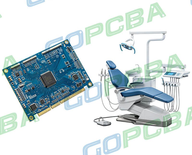
<img src="https://www.gopcba.com/wp-content/uploads/2026/05/Energy-PCBA.jpg" alt="lamination press stacking cores for a high layer count PCB” />
Inner-Layer Imaging With Special Materials
High layer count boards commonly use high glass transition temperature materials, high-speed and high-frequency laminates, thick copper and thin dielectric. Each of these makes the inner-layer imaging step harder. The fine line widths and spacings needed for dense signal layers increase the incidence of shorts and opens, and very small unintended connections become more frequent, which reduces yield. More signal layers also mean more opportunity for an automatic optical inspection system to miss a defect. Thin cores are easily wrinkled, which produces poor exposure, and they are prone to curling as they pass through the etching line. Because these boards are usually system boards with large units, a scrapped unit is expensive.
Lamination
Lamination is where the most visible defects appear, because it involves stacking many cores and prepreg sheets under heat and pressure. Slippage between layers, delamination, resin voids and trapped bubbles all occur at this step. Designing the stackup so that the process can succeed means considering the heat resistance of the material, its dielectric strength, the amount of resin available to fill the inner-layer topography, and the dielectric thickness that will result. Several rules follow. The prepreg and the core should come from the same material system, and a single sheet of the thinnest prepreg should be avoided, since one very thin layer does not provide reliable separation. Where no dielectric thickness is specified by the customer, a minimum of about 0.09 mm between layers is a reasonable floor. Where the design calls for thick inner-layer copper, a high-resin-content prepreg is needed so that the resin can fill the pattern, while a stack composed entirely of the thinnest high-resin sheets should be avoided because the fine glass yarn collapses under pressure and degrades dimensional stability and delamination performance. Unless the customer specifies otherwise, dielectric thickness is normally held within about ten percent, and for impedance-controlled boards the tolerance follows the tighter grade of the laminate specification so that the impedance target remains achievable. The reliability consequences of getting this wrong are not subtle: a board that delaminates under thermal stress test fails before it ever reaches a customer.

Drilling and Back Drilling
Drilling becomes more difficult with high glass transition materials, high-speed laminates and thick copper, because all three increase hole wall roughness, burr formation and the difficulty of desmear. The accumulated copper thickness and the total board thickness make the drill more likely to break, and the dense ball grid arrays used on these boards bring holes close together, which raises the risk of conductive anodic filament growth between them. A thick panel also tends to produce holes that are not perfectly perpendicular, and that deviation grows with depth. High aspect ratio holes, around 12:1, are usually drilled in steps from both sides of the panel to keep the drilling load reasonable. Hole wall roughness should be kept within about 25 micrometres, and the cutting tools should be new or at most reground once, because a worn drill produces exactly the roughness and burrs the process is trying to avoid. A high-density backing board and single-piece stacking help control burrs on thick copper panels. For boards that carry high-frequency or high-speed signals, back drilling is the standard method of shortening the unused portion of a through hole, and it requires a machine with the depth-control capability to remove the stub without touching the layers that must remain connected; the tolerance on the residual stub length and the alignment between the two drilling operations are what determine whether the technique helps.
Impedance Control Across a Thick Stack
Impedance control on a high layer count board is a stackup problem before it is a routing problem. The dielectric thickness tolerance, the copper weight and the material’s dielectric constant all vary, and the allowed variation becomes tighter as the board gets thicker. Where the design depends on a specific impedance, the material grade and the thickness tolerance have to be specified to a matching standard, and the trace geometry has to be calculated from the nominal values with the variation accounted for. Specifying a stackup and then asking the shop to hold an impedance that the stackup cannot support is one of the more common causes of a redesign after the first article.
Reliability Testing
A high layer count board is usually a system board, which means it is thicker and heavier than a conventional board and has a larger thermal mass. During soldering it needs more heat and spends longer above the liquidus temperature of the solder; for a tin-silver-copper alloy, a dwell of roughly 50 to 90 seconds above 217 degrees Celsius is typical, and the board also cools more slowly. Reliability testing therefore has to reflect a longer thermal excursion, and it is normally carried out against the applicable industry standards for the product class rather than against a single company procedure. The tests that matter most are thermal stress and thermal cycling, since they expose the delamination and the plated-through reliability that lamination and drilling determine.
Design Decisions That Help the Process
The designer controls several of the variables that decide whether a high layer count board can be built at acceptable yield. Keeping the unit size within the shop’s capability, avoiding a stackup built entirely from the thinnest prepreg, specifying a consistent material system, and providing adequate annular ring and hole-to-hole clearance all reduce the process difficulty. Where the density genuinely requires many layers, the decisions made about the stackup determine the result, and the options available are described in this article on layer stackup from one to eight layers. Because the same material movement that complicates registration also affects the finished dimensions, the behaviour of the laminate is worth understanding before the stackup is fixed, as described in this article on PCB dimensional stability. The via geometry that goes with these stackups is covered in this article on via design rules.
FAQ
Why is layer-to-layer registration harder on a high layer count board? Because the alignment tolerance is shared across many layers, and the movement of each core during processing is different, so the error accumulates.
Why avoid a single sheet of thin prepreg between layers? Because one very thin sheet does not provide reliable separation, and the resulting dielectric may not withstand the voltage or the thermal stress of the application.
When is back drilling used? On high-frequency and high-speed boards, to remove the unused portion of a through hole that would otherwise act as a stub and degrade the signal.