PCB Layout Constraints: Six Checks Before Placement
A board that works electrically can still be a bad board. It may not fit the enclosure, it may not panelise, it may run hotter than the thermal design assumed, or it may pass an EMC test on the bench and fail in the chamber. The checks below are the ones that are cheapest to make during layout and most expensive to discover afterwards, and together they form the practical set of PCB layout constraints for a production board.
Does the Board Shape Match the Enclosure
The first constraint is mechanical and comes from the product, not from the circuit. The outline has to fit the enclosure with the tolerance of both parts accounted for, the mounting holes have to line up with the bosses, and any connector that passes through a panel has to sit at the right height and depth. A board that is correct in every electrical respect and 0.5 mm too wide is scrap.
Check the outline against the mechanical model before placement, and re-check after, because a component that overhangs the outline is as much of a problem as a board that is too large.
Component Spacing and Height Conflicts
Components need room in three dimensions. A tall capacitor placed beside a connector may prevent the housing from closing, and a part placed too close to a neighbour may be impossible to place with the nozzle or to rework with a soldering iron. A useful habit is to draw a mechanical outline around every large component, on a mechanical layer, showing its real body size rather than the courtyard from the library, and then to treat those outlines as keepouts.
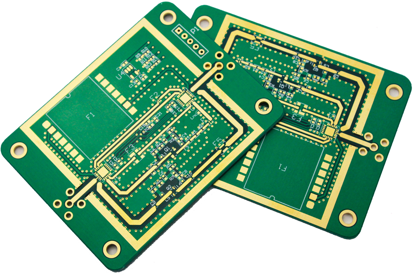
The same outlines reveal conflicts early. If two mechanical outlines overlap, the layout has a physical problem regardless of what the electrical rules say, and the fix is almost always cheaper now than after the first samples arrive.
Panelization, Process Edges and Mounting Holes
A board is not manufactured on its own; it is manufactured as part of a panel. panelization decisions affect the outline, the rails, the fiducials and the tooling holes, and they have to be made before the outline is frozen. Process edges are needed where the machine clamps the panel, fiducials are needed for the placement machine, and tooling holes are needed for every process that locates the panel.
Mounting holes have their own rules: keep them away from the board edge by more than the hole diameter, and check that the arrangement does not create a narrow cross-section that becomes the weak point of the board. Where a board is small, the panel is also a handling aid, and a small board supplied loose is more likely to be damaged than the same board supplied in an array.
Power Modules and Heat
Power conversion belongs near the point of use, but not next to anything that cares about temperature. Place the regulator close to its load to keep the current loop short, and place it away from the reference, the crystal and any precision analogue part. If a module dissipates significant power, give it copper to spread the heat into, and consider whether that heat should be steered to the board edge or into a chassis.
The connection between the power stage and the rest of the board is also worth thinking about in terms of EMC: the switching loop should be small, and the return current should have a continuous path back to the source.
Adjustable and Replaceable Parts
Parts that a technician will touch need to be accessible. Trimmers should be reachable without removing the board, connectors that are plugged and unplugged repeatedly should be at the edge, and components that fail or that are firmware-specific should be socketed or at least not buried under a shield can. Accessibility is a mechanical property of the layout and it costs nothing to design in.

Common-sense serviceability also reduces the chance of damage: a connector at the board edge takes the insertion force through the housing rather than through the solder joints, and a part that can be replaced without a hot-air station is a part that will be replaced correctly in the field.
Thermal Separation
Clearance Around the Board Edge
The perimeter of the board deserves a check of its own, because several rules converge there. Components need a keepout for the depanelling tool, copper needs a pullback from a routed or scored edge, and any trace running close to the outline will behave differently from one with solid laminate on both sides. A common working figure is 0.3 mm of copper pullback from a routed edge and 2 mm of component clearance from the outline, but both should be taken from the fabricator’s design rules rather than assumed.
Edge plating, castellated holes and connector fingers are deliberate exceptions, and each needs its own note on the fabrication drawing so that the fabricator does not apply the general rule to a feature that is meant to break it.
Heat sources and heat-sensitive parts should not be neighbours. The distance needed depends on the power dissipated and the sensitivity of the victim, but a useful rule is to keep temperature-sensitive devices at least 10 mm from anything that runs more than 20 degrees above ambient, and to keep crystals and references further away than that.
Where space does not allow the distance, use the layout to help: a slot between the two areas interrupts the conduction path in the laminate, and a local ground pour under the sensitive part spreads what remains.
EMC and ESD at Layout Time
Electromagnetic compatibility is mostly decided by the layout, not by the enclosure or the cables. Keep the high-speed loops small, keep the return paths continuous, and keep the switching nodes away from connectors and cables. Where a signal leaves the board, it is the most likely path for both emissions and incoming transients, so filters and protection belong close to the connector rather than close to the chip.
Electrostatic discharge protection has a straightforward layout rule: the protection device must be between the connector and the circuit it protects, with a short return to ground, and the trace from the connector to the device must not run past the protected circuit on the way. ESD and PCB edge traces explains why the routing near the board edge matters so much.
Where the Outline and the Rules Meet
Several of these constraints meet at the board edge. The mechanical outline sets where copper must stop, the panelization scheme sets where components may not go, and the EMC requirements set how close a trace may run to the edge. Board outline and mounting design brings these together, and EMI suppression design principles covers the layout measures that reduce emissions without adding components.
FAQ
When should the mechanical drawing be reviewed? Before placement starts and again before the board is released. The second review catches components that grew or moved during layout.
How much spacing should be left between components? Enough for the placement nozzle, the rework tool and the thermal separation the design needs. The assembly house can give a minimum; the thermal requirement is usually larger.
Is panelization the designer’s problem? The panel is the fabricator’s decision, but the outline, the rails and the keepouts that make it work are the designer’s. Agreeing the panel scheme early avoids an outline that cannot be arrayed efficiently.