PCB Production Process Complexity: Why Board Builds Get Hard
Printed circuit board manufacturing is unusual among production processes in that it combines mechanical machining, photochemistry, electrochemistry, heat and pressure, and computer-aided data preparation in a single flow. Each step is only as good as the one before it, the work in process cannot be stored indefinitely, and a defect introduced at the start may only become visible at the end. That combination is what makes the PCB production process difficult to control and expensive to get wrong.
Why Complexity Grows With the Circuit
The more complex the product, the longer the signal paths and the greater the number of connection points, and the more layers the board needs to carry them. Each additional layer adds a lamination cycle, another set of registration tolerances and another opportunity for a defect that will not be found until the electrical test. Complexity is therefore not a property of the artwork alone; it is a property of how many times the panel has to be processed.
What the Process Actually Involves
The sequence spans a wider range of disciplines than most people expect. There is mechanical work in cutting, drilling and profiling. There is photochemistry in the imaging of the resist. There is electrochemistry in the plating of the holes and the surface finish. There is heat and pressure in the lamination. And there is a substantial data preparation step, where the customer’s design files are converted into tooling data for every machine on the line.
Because the flow is a continuous line rather than a batch process, an interruption at one station stops everything downstream. A panel that fails at the end of the flow has consumed the value of every step, and the material cannot be recovered.
The Conductor Pattern
The copper that remains after etching is the conductor pattern, the network of lines that connects the components. On a simple single-sided board the pattern is on one face and the parts are on the other, which is why that construction needs holes: the leads pass through the board and are soldered on the opposite side.
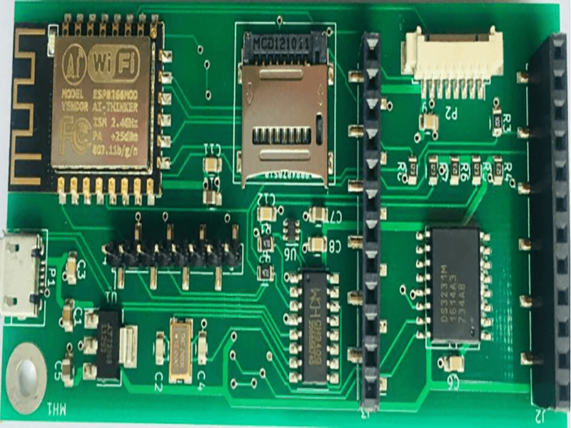
The two faces of a single-sided board are traditionally called the component side and the solder side, and the naming still appears in design tools even where the board is far more complex than that. Understanding which face a part is on and which face it is soldered from is the basis of every assembly drawing.
Component Sides and Assembly
Assembly is where the board meets the components, and the sequence is set by the soldering process. Surface mount parts are placed on paste and reflowed; through-hole parts follow on a wave or selective solder process. Where the design places parts on both sides, the board passes through two reflow cycles, and each cycle is a thermal stress event that the laminate has to survive.
Sockets are used where a component has to be removable, either because it is programmed, because it is a consumable, or because it may fail. The socket is soldered to the board and the component is inserted afterwards, which means the socket’s own solder joints carry the insertion and extraction forces over the life of the product.
Edge Connectors and Gold Fingers
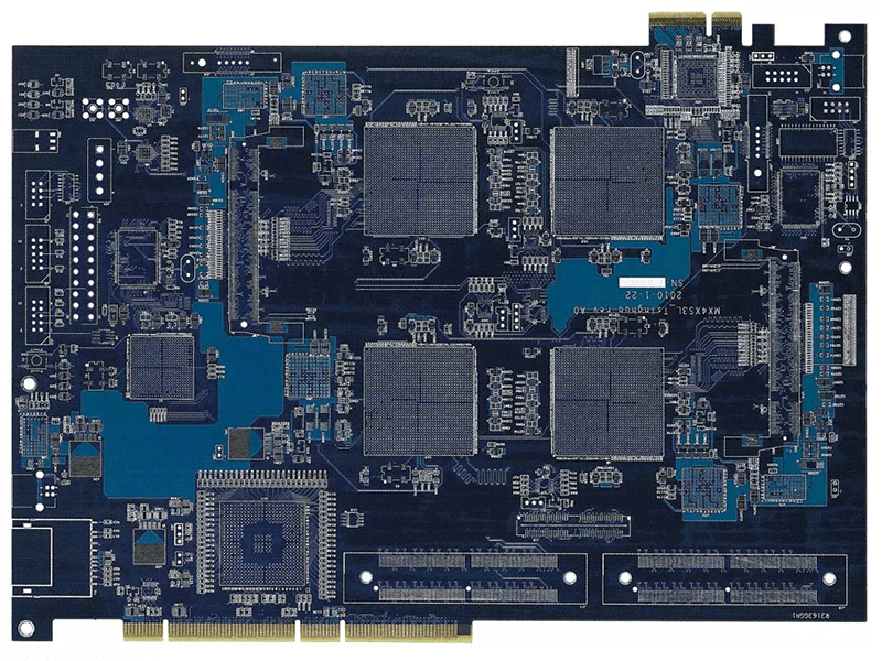
A board that plugs into another board or into a backplane uses an edge connector, and the contact surfaces are the plated tabs commonly called gold fingers. They are part of the conductor pattern, extended to the board edge and plated with a hard finish so that they survive repeated insertion.

The fabrication requirements for a plug-in edge are specific: the fingers need a defined width and spacing, the bevel angle has to suit the mating connector, and the finish thickness has to be controlled because it contributes to the final height of the tab. A board that is otherwise perfect can be rejected for a bevel that is out of specification.
Panel Handling and Breakage
Panels are handled many times between the first cut and the final packing, and each handling step risks a scratch, a nick or a fracture at a thin section. Boards with narrow necks, large cut-outs and small overall size are the most exposed, which is why they are usually shipped in an array with rails until the last possible moment.
The outline and the panel design therefore have a direct effect on yield, and they are worth agreeing with the fabricator before the design is released. PCB design and fabrication working together is mostly about making these interfaces explicit.
Where Process Problems Come From
Problems in a process this long rarely have a single cause. A specific fault, such as a break where the laminate is recessed, may point to contamination on the press plates. A concentration of fine-line defects in one area of a panel may point to a vacuum problem in the exposure unit. Faults that cluster on one part number usually indicate a conflict between the customer’s design rules and the shop’s process capability.
Faults that appear at random are the hardest to resolve, because they may require equipment or tooling investment rather than a process adjustment. Separating these categories, and being honest about which one a given defect belongs to, is the core of process engineering.
Yield Data and Why It Matters to a Designer
Yield data is the feedback signal from the process, and it is worth asking for even when a design is being prototyped. A design that yields 95 percent on a first build is comfortable; one that yields 60 percent will cost more in production than the design savings that caused it. The causes are usually predictable once the data is available: marginal line width, insufficient annular ring, or copper distribution that makes the panel press unevenly.
That is why the most experienced designers keep their design rules close to the fabricator’s standard capability rather than at the edge of it. PCB design quality characteristics describes the evidence that supports that judgement.
FAQ
Surface Finish and Its Process Window
The surface finish is chosen for solderability and shelf life, and each option constrains the process in a different way. An organic coating is simple to apply and flat, but it has a short storage life and cannot be handled carelessly. An immersion finish is more durable and more expensive. A hard gold finish on connector tabs must be applied selectively, which usually means an extra imaging and plating step that has to be planned into the panel flow rather than added afterwards.
Finish selection also interacts with the assembly process. A finish that is perfectly adequate for a board assembled within weeks may be unsuitable for one that will be stored for a year before use, and the choice should be made with the storage and handling plan in mind rather than on solderability alone.
Inspection and the Cost of Late Detection
Inspection points are placed where the value added so far is still small enough that scrapping is tolerable. Inner layers are inspected after etching, outer layers after etching, and the finished panel after coating and finish. Each inspection catches what the previous step introduced, but it cannot catch a defect that will only appear later, such as a marginal hole wall that passes continuity testing and fails in thermal cycling.
That is why qualification work matters as much as inspection. A microsection from a first article, a thermal stress test and an impedance measurement give information that a continuity test cannot, and they are the tools that turn a process from one that usually works into one that is understood.
Why is PCB manufacturing harder to control than other assembly work? Because it is a continuous line of dissimilar processes with accumulated tolerances. A defect can pass through every station and only be detected by electrical test at the end.
What is the single biggest driver of layer count? The number of connection points and the routing density between them. More components and more nets means more layers, which means more lamination cycles and more process risk.
How can a designer help the fabricator? Stay within the published design rules, keep the copper distribution balanced, agree the panelization early, and provide a complete data package with the stackup and impedance requirements stated. Multilayer PCB advantages in high speed designs is a useful reminder of what the extra layers are buying.