PCB Production Process: From Cutting and Drilling to Final Test
A printed circuit board starts as a sheet of copper clad laminate and ends as a tested substrate with copper features measured in tens of microns. The PCB production process between those two points is a sequence of additive and subtractive steps that alternate between chemistry and imaging, and understanding that sequence makes a layout engineer far better at writing manufacturing notes.
The steps described here are the core flow for a rigid multilayer board. Heavy copper, high frequency laminates, flex and metal core substrates all change the details, but the order of operations stays recognisable.
Cutting and Inner Layer Imaging
Cutting is not simply trimming the panel to the finished outline. The laminate is sheared to a working panel size that matches the machine envelope, then a cutting plan is drawn to maximise the number of boards that fit while leaving room for tooling holes and process coupons. Material utilisation is a real cost driver, especially on high layer count or specialised laminates, so the panel layout is optimised before the first hole is drilled.
Inner layers are then coated with photoresist, exposed through the artwork and developed, leaving resist only where copper must remain. Etching removes the exposed copper and the resist is stripped, producing the inner layer pattern. Each inner layer is inspected for opens, shorts and line width before it is committed to lamination.
Line width tolerance at this stage sets the achievable impedance tolerance at the end of the process. A design that calls for a tightly controlled differential impedance has to allow for the etch variation the fabricator can actually hold, so the stackup and the trace geometry are agreed before the inner layers are imaged rather than after the first measurement.
Lamination and Drilling
The inner layers are stacked with prepreg between them, copper foil on the outside, and pressed under heat and pressure until the resin flows, cures and bonds the stack into a single rigid panel. Registration between layers is set at this step and cannot be corrected later, which is why the layer to layer alignment budget is one of the more important numbers in the fabrication drawing.
Drilling follows. Holes carry signals between layers, provide mounting and tooling references, and set the size of the vias in the design file. Drill diameter, hit count and stack height are chosen together, because a worn bit cuts a smaller hole and a stack that is too tall loses positional accuracy. After drilling the panel is deburred and the hole walls are prepared for plating.
Hole quality is judged on the microsection rather than on the drill log. A nail head at the copper entry, resin smear on the inner layer pad or a cracked barrel all point to a drill parameter that needs adjustment, and all three reduce the long term reliability of the connection even when the board passes a continuity test.
Electroless Copper and Pattern Plating
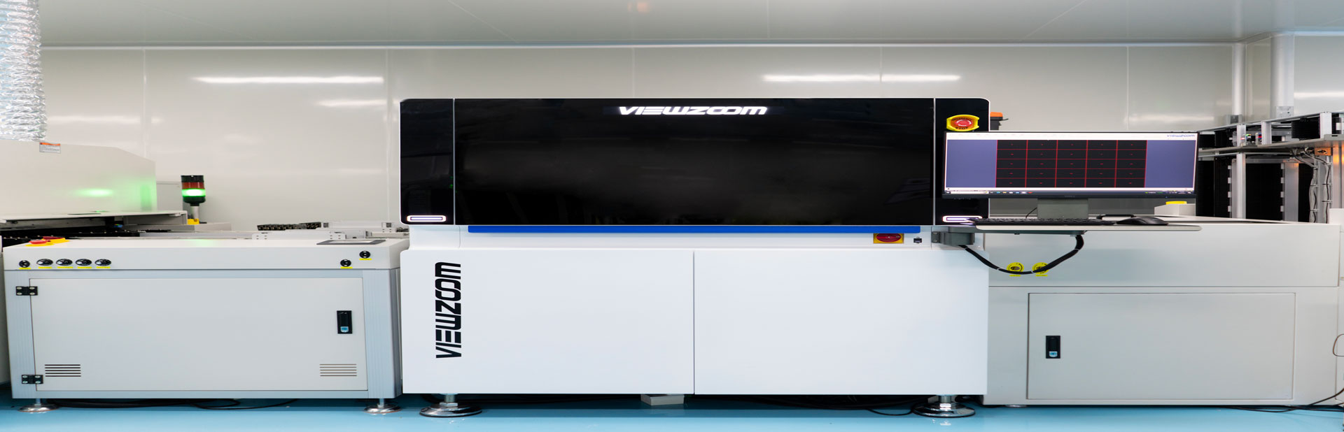
The laminate has no copper inside the holes, so a conductive path must be created before electroplating can build thickness. That is the job of electroless copper: a catalysed chemical deposition that lays a very thin, continuous layer over the hole wall and the panel surface, typically 0.05 to 0.1 mil. The layer is far too thin to carry current, but it makes the surface conductive so the plating line has something to work with.
Pattern plating then adds copper where the circuit requires it. The panel is imaged with a plating resist that exposes only the traces, pads and hole barrels, and copper is electrodeposited to the finished thickness. Tin is plated over the copper as an etch resist in the same step. Because the resist openings define the pattern, plating thickness varies with the local current density, so thieving bars and shields are used to even out the distribution across the panel.
Etching and Resist Stripping
Once plating is complete, the tin resist is stripped from the non-circuit areas and the exposed copper is etched away. The tin protects the plated traces from the etchant, so the copper that remains is exactly what was plated. Etch factor, the ratio of lateral undercut to vertical etch depth, determines how faithfully the trace width in the design is reproduced; it is controlled by chemistry, conveyor speed and the uniformity of the spray.
Solder Mask and Legend
Solder mask is applied as a photoimageable layer, exposed and developed so that the openings land on the pads that must be soldered. Its functions go beyond protection: the mask prevents solder bridging between fine pitch pads, keeps the surface insulation resistance high under humidity, and defines where rework is possible. Openings are usually made slightly larger than the pad to allow for registration error, which is why the mask web between two pads is the limiting feature on a fine pitch design.
Legend is printed after the mask, by screen printing or inkjet, and cured. Text has to stay clear of pads, and the reference designator orientation should be readable from one direction so that assembly and inspection are not slowed down by rotated labels.
Surface Finish
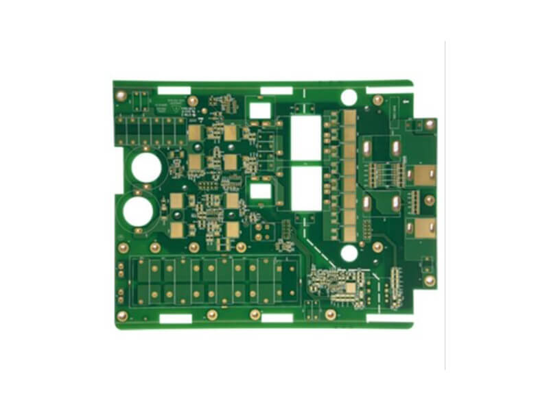
The exposed copper on pads and connector fingers then receives a finish that keeps the surface solderable. Hot air solder levelling applies a thin solder coating and is inexpensive but has a higher thermal load on the panel. Electroless nickel immersion gold gives a flat surface that suits fine pitch and wire bonding. OSP is an organic layer that protects copper during storage and disappears during the first reflow. Immersion silver and immersion tin fill other niches, and the choice is normally driven by storage life, the number of reflow cycles and the soldering process.
Which finish suits a given product is covered together with the wider fabrication sequence in the notes on PCB design and fabrication and on multilayer prototype requirements.
Profiling and Electrical Test
Profiling cuts the working panel into individual boards with a router, a V-score or a punch, depending on the outline and the panel design. V-scoring leaves a controlled groove that allows the boards to be separated after assembly, while routing gives a clean edge with cut-outs and slots.
The final gate is electrical test. A flying probe or a bed of nails fixture checks every net against the netlist for opens and shorts, and the panel is also inspected for cosmetic and dimensional compliance. Boards that pass are packed with a desiccant and a humidity indicator before shipment. For a first article, a coupon from the same panel is also microsectioned to verify plating thickness, hole wall quality and layer registration, which is the only way to see inside a finished board. The fundamentals of what the board is doing electrically in the first place are covered in the overview of the printed circuit board.
Flying probe and fixture test serve different purposes. A fixture is fast and pays back quickly on volume, but the tooling cost has to be justified. A flying probe needs no fixture and can be programmed in hours, which is why it dominates prototype and small batch work even though it is slower per board. Where the design contains impedance controlled nets, the coupon is also measured for characteristic impedance, since that property cannot be verified from the test netlist at all.
FAQ
Why is electroless copper needed if the board is electroplated later? Electroplating requires a conductive surface. Electroless copper provides that seed layer on the non-conductive hole wall.
How long does a multilayer board take to produce? A standard multilayer order is measured in days. Layer count, surface finish, impedance requirements and tooling all add time, so the schedule should be agreed before the data is released.
Is electrical test enough to confirm a board is good? It confirms connectivity. Plating thickness, hole wall integrity and dielectric spacing are verified separately with coupons and microsections.