
PCB Design Layers Explained: Signal, Plane, Mask, and Mechanical
Modern layout software presents the design as a stack of named layers, and new engineers often find the number of them overwhelming. Each layer has a specific role, and each one produces a different output file or a different instruction to the fabricator. Confusing them is not a cosmetic problem: putting board geometry on the wrong layer, or using the wrong layer as a boundary, changes what the fabricator builds. This guide explains the PCB design layers that appear in a typical design and what each one actually does.
The layers fall into three groups. Some describe the copper that becomes the circuit, some describe the coatings and markings applied over it, and some are documentation layers that exist only in the data package. The middle group is where most mistakes occur, because those layers modify how the copper is protected rather than where it is.
Mechanical Layer
The mechanical layer carries the physical description of the board: the outline, the dimensions, the position of mounting holes, the alignment features, and any assembly notes. It is a documentation layer in the sense that it does not become copper, but it defines what the finished board looks like and where it fits.
Its accuracy determines whether the board can be assembled into its enclosure. The outline on this layer is used to produce the profile routing program, so an error here becomes a physical board that does not fit rather than a manufacturing defect that can be corrected. Where the design includes features such as slots or cut-outs, they are dimensioned on this layer as well, and the constraints of that geometry are covered in board outline and mounting design.
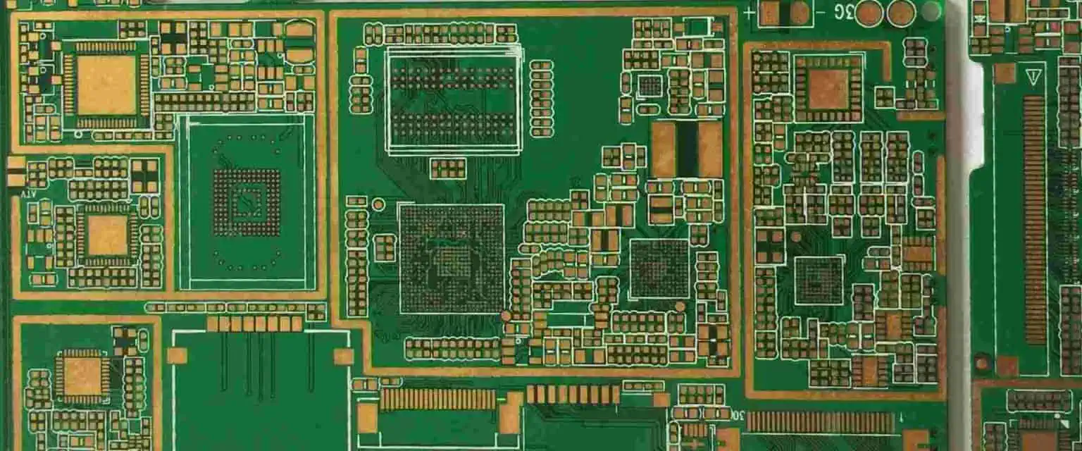
Where a design has more than one mechanical layer, the fabricator still needs an unambiguous statement of which one defines the profile. That information belongs in the fabrication drawing rather than only in the layer name.
Keep-Out Layer
The keep-out layer defines the region in which components and conductors may be placed. A closed boundary drawn on this layer marks the valid routing area, and anything outside it is excluded from automatic placement and routing.
The important point is that the keep-out layer is not a mechanical layer. The two are frequently used interchangeably, and the result is a data package where the boundary is ambiguous; some fabricators will silently correct the layer, others will build what the file says. Keeping the two distinct prevents the ambiguity.
Keep-outs are also used locally, around mounting hardware, inside cut-outs, and around features that must not be disturbed. Each local keep-out is a constraint that the design rules enforce, so a late change to the outline must be reflected in the keep-outs as well.
Signal Layers
Signal layers carry the conductors that form the circuit. A typical design has a top layer, a bottom layer, and one or more internal signal layers, numbered consecutively. Components are normally placed on the top and bottom layers, while the internal layers carry routing that connects them.
Each signal layer has a reference plane associated with it, usually the nearest adjacent plane, and the impedance of a controlled trace is determined by its width, its thickness, and its distance to that reference. That is why the stackup order matters as much as the number of signal layers, and why two designs with the same layer count can behave very differently. The relationship between layer assignment and impedance is described in layer stackup from one to eight layers.

On multilayer designs the internal signal layers are numbered from the top down, and the numbering convention must match the stackup drawing. A mismatch between the layer numbering in the CAD file and the stackup document is a common source of registration errors during data preparation.
Paste Layers
The top and bottom paste layers define the aperture in the stencil through which solder paste is printed. The opening on this layer corresponds in size to the component pad, so the printed deposit lands on the pad with the intended volume and shape.
The paste layer is used to generate the stencil, and the stencil is what actually deposits the paste. Because the aperture size controls the volume of solder, any deviation between the paste layer and the pad is a deviation in the joint. Where a design calls for a reduced or enlarged deposit, that adjustment is made on this layer rather than on the copper, so the copper geometry stays within the design rules.
Solder Mask Layers
The solder mask layer defines the openings in the protective coating. By default, copper features are covered by mask; drawing on this layer removes the coating from a specific area, exposing the copper so that it can be soldered or contacted.
Two rules govern its use. The openings should be larger than the pads by a defined clearance so that the mask cannot overlap the solderable area, and the mask remaining between adjacent openings, the dam, must be wider than the process can print. Where the geometry cannot support a dam, the correct action is to open the mask across the row rather than to specify a dam that will break down. Coating behaviour is described in solder mask design.
Internal Plane Layers
An internal plane is a layer that consists of continuous copper rather than routing, and it is used for power distribution and for the ground reference. Planes are normally used only on multilayer boards, and the layer count quoted for a board refers to the total of signal and plane layers together.
A plane may be divided into regions to carry more than one supply voltage. Each division interrupts the return path for any signal referenced to that plane, so a signal should not be routed across a split. The mechanics of that constraint, and how to arrange the regions, are described in power plane splitting rules.
Silkscreen Layer
The silk layer carries the printed markings: component outlines, reference designators, polarity indicators, and notes for assembly. It has its own minimum line width and character height, and text below those limits is unreadable after printing.
The layer should be reviewed for legibility rather than for completeness. A designator printed under a component body, or across a pad, is worse than one moved to a different position, because the first is invisible and the second is merely inconvenient.
Multi Layer
The multi layer is an abstraction rather than a physical layer. Pads and through-hole vias exist on every copper layer that they pass through, and placing them on the multi layer is what makes them appear on all of them. Turning the multi layer off in the display therefore hides every pad and through-hole via in the design, which is a common source of confusion when a layout appears to have lost its pads.
Objects on this layer must be treated carefully, because a change made here affects every layer at once. The layer is also the reason through-hole pads enlarge the drill count and consume routing space on every layer they pass through, which is the underlying motivation for moving to blind and buried structures on dense boards.
Drill Drawing and Documentation Layers
The drill drawing describes the holes to be produced: their positions, their diameters, and whether they are plated. It is the document from which the drilling program and the drill chart are derived, and it is also what the fabricator uses to verify that the drill data matches the artwork.
Additional documentation layers carry assembly information, dimensions, and notes. These do not affect the fabrication of the bare board but are essential to the assembly house, and they should be included in the released package rather than stored separately. The overall structure of the board and its copper is described in the PCB circuit board explained.
FAQ
Is the keep-out layer the same as the mechanical layer? No. The mechanical layer describes the physical shape of the board, while the keep-out layer defines where components and conductors may be placed. Using one for both purposes creates ambiguity in the data package and should be avoided.
What happens if the paste layer differs from the pad? The stencil aperture changes, and therefore so does the volume of solder printed. A larger aperture produces excess solder and possible bridging, a smaller one produces insufficient solder and a weak joint. The two layers should always be generated from the same pad definition.
Why do pads disappear when I turn off the multi layer? Because pads and through-hole vias are placed on the multi layer so that they exist on every copper layer. Hiding that layer hides all of them at once, which is a display behaviour rather than a change to the design.