High-Speed PCB Design Basics: Stackup, Bends, and Via Transitions
High-speed design is often presented as a collection of rules without an explanation of why they exist. The underlying model is straightforward: a conductor carrying a fast edge is a transmission line, its return current follows the reference plane beneath it, and any change to that geometry produces reflection, radiation, or coupling. Once that model is accepted, the standard practices follow from it. This article covers the high-speed PCB design basics that connect the rules to the mechanism.
Three properties distinguish a high-speed design from a slow one. The edges are fast enough that the physical dimensions of the board matter relative to the wavelength of the signal content. The return path therefore has to be designed rather than assumed. And the tolerances that are invisible at low frequency, such as a stub or a mismatched segment, become significant contributors to the result.
Why Multilayer Construction Helps
The most effective single measure is to route fast signals in a multilayer board with continuous reference planes. A plane provides a defined return path beneath the signal, which keeps the loop area small, reduces the parasitic inductance of the interconnection, and allows the trace impedance to be controlled and predicted.
The internal layers are also partially shielded by the planes around them, which reduces radiated emission compared with a trace on an outer layer. Reported comparisons put the noise difference between a four-layer and a two-layer construction of the same circuit on the order of 20 dB, which is consistent with the difference between a defined return path and an undefined one.

The layer count should be chosen for the routing requirement rather than fixed in advance. Adding layers costs money, but an inadequate stackup costs signal integrity, and a stackup that cannot provide a reference plane under every fast signal will not be rescued by additional decoupling.
Layer Stackup and Adjacency
Two adjacent signal layers are a problem, because they couple to each other and neither has a reference plane on both sides. Where the stackup forces two signal layers to be adjacent, their routing directions should be perpendicular so that the parallel run length between them is minimized.
A six-layer stackup can be arranged with two internal routing layers and reference planes, and an eight-layer stackup provides more freedom to give every signal layer an adjacent plane. The best arrangement puts the fastest signals on the layers that are closest to a solid plane and keeps power and ground as continuous as the routing allows. The principles governing plane arrangement are described in layer stackup from one to eight layers.
<img src="https://www.gopcba.com/wp-content/uploads/2026/08/HDI-PCB-design.jpg" alt="Differential pair routing with guard traces on a high speed board” />
Ground and power planes should be tightly coupled to each other and to the signal layers around them. Reducing the dielectric thickness between a signal layer and its reference widens the trace for the same impedance, which reduces both loss and crosstalk.
Bends, Corners, and Radiated Emission
A change of direction on a fast trace is a discontinuity. A ninety degree corner concentrates the electric field at the inner edge, which produces a local change in impedance and a small amount of radiation. The rule is therefore to avoid sharp corners: use a straight section wherever possible, and where a turn is unavoidable use a pair of 45 degree segments or a smooth arc.
The improvement is modest for a single corner but accumulates over a long route with many turns, and it is easiest to apply while the routing is being drawn rather than as a cleanup afterwards. The same reasoning applies to the transition between a trace and a pad, where a sharp geometry can produce a similar local discontinuity.
Trace Length and Distributed Effects
Short interconnections are better for the same reason that they are easier to route: the longer the conductor, the larger its distributed inductance and capacitance, and the more it behaves as a transmission line rather than as a wire. Lengthening a connection between two devices increases delay, adds reflection at the impedance transitions, and makes the circuit more sensitive to the characteristics of the driver and the receiver.
The practical rule is to place devices so that the critical connections are short, then route them directly. Where a length cannot be reduced, the trace must be designed as a controlled-impedance line with a defined reference and terminated appropriately, because an uncontrolled line behaves differently depending on its length and the source impedance.
Via Transitions and Their Cost
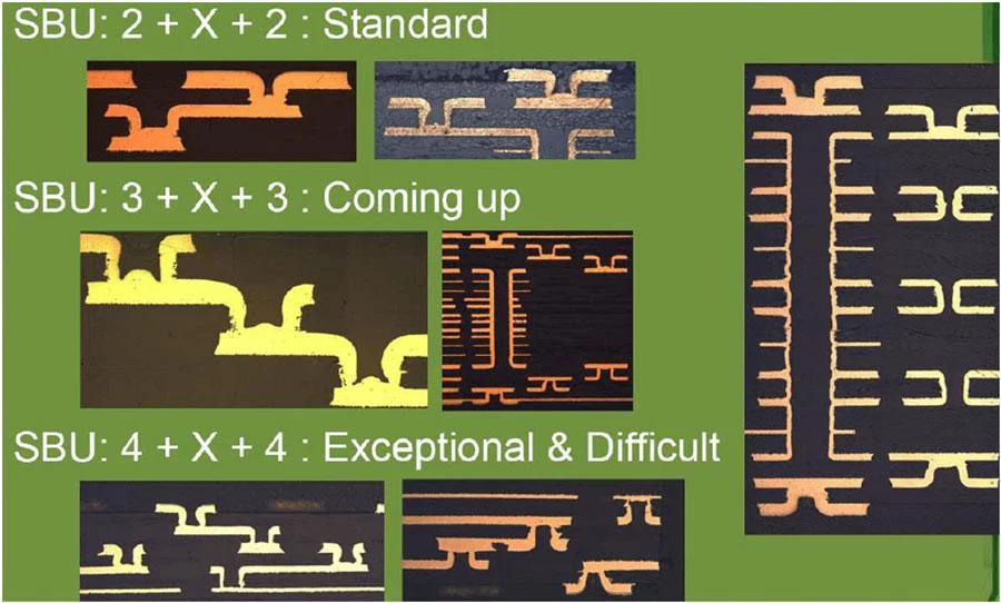
Every layer change introduces a via, and a via is not electrically transparent. A typical through-hole via adds roughly 0.5 pF of distributed capacitance, and that capacitance loads the line and increases the propagation delay. The deeper the via, the longer the unused portion of the barrel, which behaves as a stub that resonates at a frequency determined by its length.
The rule is therefore to minimize the number of layer transitions on fast nets, and to keep the remaining vias short. On a thick board, back-drilling the stub or using blind and buried structures removes the unused barrel. Where a transition is unavoidable, a return via should be placed adjacent to the signal via so that the return current can change reference planes at the same point.
Parallel Routing and Crosstalk
Two conductors that run alongside each other couple energy through their mutual capacitance and inductance, and the longer the parallel run, the more energy transfers. The coupling increases with the proximity of the traces and with the rate of change of the aggressor’s current, which is why fast signals are the usual aggressors and sensitive signals the usual victims.
Where parallel routing cannot be avoided, a ground plane placed on the opposite side of the board beneath the parallel section intercepts part of the field and reduces the coupling. Increasing the spacing between the two traces is usually more effective and costs only routing area, which is the basis of the widely used spacing rules described in the 3W crosstalk rule. Routing on adjacent layers should be perpendicular rather than parallel, so that the two traces cross rather than run together.
Guarding Critical Signals
A particularly sensitive trace, such as a clock or a high-speed analog line, can be enclosed by ground conductors on both sides, with the protected trace sandwiched in the middle. The guard conductors are connected to the reference at intervals, and they intercept the field that would otherwise couple into the victim.
The guard structure has a second benefit: it prevents the routing from forming a loop. A conductor that leaves a device and returns to it through a different path creates a loop, and a loop is an efficient antenna both for emission and for reception. Guarding keeps the geometry controlled and avoids the accidental loop.
Decoupling and Ground Separation
Every integrated circuit needs one or more high-frequency decoupling capacitors close to its supply pins, because the supply network cannot deliver current fast enough to satisfy the switching transient. The capacitor supplies the charge locally, and its effectiveness depends on the inductance of the path between it and the device, which is why placement and via arrangement matter as much as capacitance value.
Where analog and digital grounds meet at a common reference, the connection should be made through a component that limits high-frequency coupling rather than through a direct short. Ferrite beads or similar elements are used for this purpose, so that the low-frequency reference is common while the high-frequency noise generated by the digital section does not propagate into the analog ground. The return path planning that supports this arrangement is described in ground routing and power trace planning.
Differential Pair Routing
A differential pair carries equal and opposite currents, so the fields of the two conductors largely cancel and the pair radiates less than a single-ended trace carrying the same signal. The benefit depends on symmetry: the two traces must be on the same layer, kept at constant spacing, and matched in length.
No other signal should be routed between the two conductors of a pair, because doing so breaks the coupling and converts part of the differential signal into a common-mode component that radiates. Length matching matters because any difference in propagation delay between the two conductors also converts differential energy into common mode. Where matching is required, the tuning pattern should use long segments with generous spacing rather than tight serpentine turns, as described in high-frequency trace and data bus routing.
FAQ
Do I need a multilayer board for every high-speed design? Not for every design, but a continuous reference plane is essential for any signal whose edge rate makes the return path significant. A four-layer board with a solid ground plane is the practical minimum for a design with fast digital interfaces, and a two-layer board can work only at lower speeds or with very short connections.
How much does a single via really matter? A single via adds a fraction of a picofarad, which is negligible on a slow net. On a fast net, the capacitance plus the stub effect of the unused barrel produces a measurable impedance discontinuity and additional delay, and the effect accumulates with every additional transition along the route.
Why is a ground plane opposite a pair of parallel traces helpful? Because it provides a return path that is close to both conductors, which reduces the loop area and intercepts part of the field that would otherwise couple between them. The plane does not eliminate crosstalk but reduces it, and it works best when combined with increased spacing.