



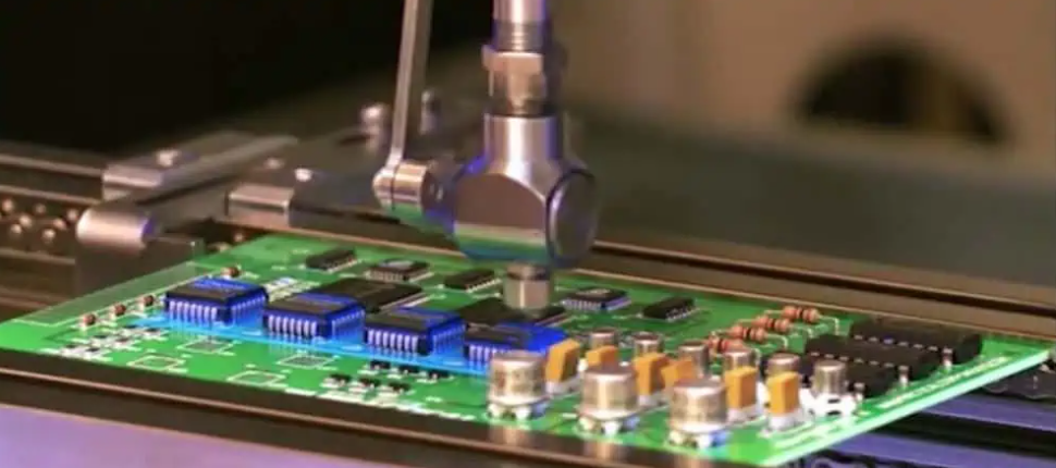
Non-Isolated Switching Supply PCB Layout: Rules That Matter
A prototype power board that works quietly and runs cool on the first power-up is a rare outcome. More often the board functions, but the switching waveform jitters, a magnetic component buzzes in the audio band, or the output carries ripple that no amount of compensation removes. The cause is frequently the layout.
Layout decides whether the current conduction path is short and tight or long and inductive, whether the control circuitry sees clean ground or switching noise, and whether heat leaves the power devices or builds up under them.
Plan the Board Before Placing Parts
On a large system board, an embedded converter needs to sit close to its load. Every inch of copper between the supply and the load adds impedance and voltage drop that no feedback loop can remove. If forced air cooling is available, the supply belongs near the fan, not in a still corner.
Plan the space early. Power management is often treated as a detail added after the interesting circuits are placed, and the result is a converter squeezed into whatever area remains, with long input loops and no room for thermal copper.
<img src="https://www.gopcba.com/wp-content/uploads/2026/06/Collaborative-Robot-Controller-PCBA.jpg" alt="Non-isolated switching supply board with power stage layout” />
The Current Conduction Path Comes First
Every switching supply has loops that carry pulsed current. The critical one is the input loop formed by the input capacitor, the high-side switch and the return path. Its area should be as small as physically possible, because loop area sets radiated emissions and the amplitude of switching noise coupled into nearby circuits.
Trace the current conduction path on paper before routing. High di/dt paths must be short and wide. The output loop matters too, but it carries smoother current, so its geometry is less critical than the input loop.
Keep the ground return of the power stage separate from the small-signal ground and join them at one point under the controller. This keeps switching currents out of the feedback divider and the compensation network, which is where they do the most damage.
Power Stage Layout
Divide the circuit into the power stage, which carries the high currents, and the control section, which senses and regulates. Place the power stage components first, then position the control circuitry around access points that the layout provides.
Input and output capacitors belong at the pins of the devices they serve, not at the far end of a plane. High-frequency decoupling capacitors should be ceramic with low effective series inductance, chosen from dielectric types that hold capacitance over voltage and temperature.
Where no heatsink is used for a surface-mount MOSFET and inductor, the copper area under and around the parts must be sized for the heat they generate. Thermal vias under the exposed pad carry heat to the internal or bottom copper, and several small vias outperform one large one.
Ground and Plane Strategy
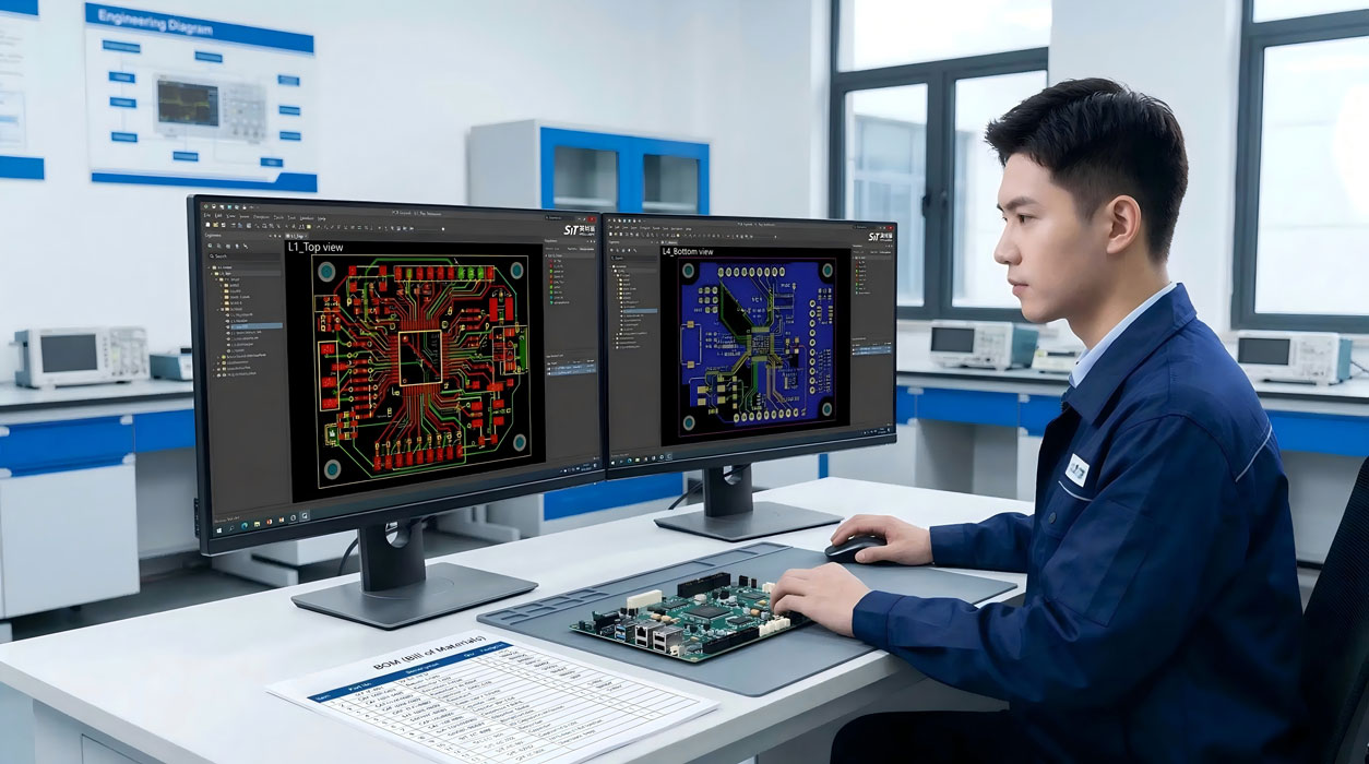
A multilayer board should use one layer as a continuous ground or DC voltage plane. That plane provides a low-impedance return path and shields small-signal traces from the switching node and the power components. It should not be split for convenience.
If a plane must be divided, keep the number and length of traces crossing the split to a minimum and route them parallel to the large currents so that the induced effect is at least predictable. A split under a feedback trace converts a precision node into an antenna.
Thermal Stress and Component Life
Thermal stress shortens life even when the circuit still functions. Electrolytic capacitors lose life roughly by a factor of two for every ten degrees Celsius of temperature rise, so keeping them away from the inductor and the switch is a reliability decision, not a cosmetic one.
Group the heat sources together so that hot spots are predictable, then keep temperature-sensitive parts outside them. Copper area, via count, board thickness and airflow all change the junction temperature of a power device more than the ambient temperature does.
Containing Switching Noise
The switching node is the noisiest net on the board, and its copper should be no larger than necessary. A large switch node pad acts as a capacitor plate and couples noise into any conductor above or below it, including the plane on the next layer.
Keep the feedback trace short and away from the inductor. Route it on the opposite side of the board if the layout allows, and never run it under the switch node or parallel to the gate drive. Sensitive analog traces belong on the far side of a ground plane, not beneath the supply.
Placement Details That Decide Performance
Inductors are the largest magnetic field source on the board, so their orientation relative to neighboring inductors and sensitive loops matters. Two inductors placed side by side can couple; rotating one by ninety degrees reduces that coupling noticeably.
Keep high-current output paths away from the sense point. Solder the sense connection directly at the load or the output capacitor terminal, not on a trace that also carries the load current, or the regulator will correct for a voltage drop that does not exist at the load.
Layer Count and Return Path Choices
Two-layer switching supplies can be quiet if the ground return is planned as a real conductor rather than a collection of traces. Route the power stage on the top layer with a wide ground area beneath it, and keep the control section over the same ground so the return paths stay short and predictable.
Four layers make the job easier: one layer for the power stage, one for a continuous ground plane, and the remaining space for control and feedback routing. The extra cost is usually less than the engineering time spent chasing noise on a two-layer board that was never laid out for it.
Checking the Layout Before Release
Review the layout against five questions: how large is the input loop, where does the power-stage ground join the signal ground, how much copper surrounds each heat source, is the feedback trace shielded from the switch node, and does the switch node copper exceed what the current requires.
A layout that answers those five questions is usually quiet. The remaining issues, such as output ripple or load transient response, are then circuit problems with circuit solutions rather than layout problems hiding behind a compensator.
Related material: radiated EMI in regulator layout, DC-DC converter layout and routing, and ground routing and power trace planning.
FAQ
Why does my inductor make an audible noise? Pulsing in the audio band excites the winding and core mechanically. Check whether the converter is entering pulse-skipping or burst mode at light load, and whether the control loop is marginally stable under those conditions.
Can I use a solid plane as the power stage ground return? Yes, and it is usually the best choice on a multilayer board, provided the small-signal ground connects at one controlled point. The failure mode is not the plane but multiple uncontrolled return paths between power and signal ground.
How much copper does a power device actually need? Enough to keep the junction temperature inside its rating at the worst-case ambient. Calculate from the thermal resistance of the package and the copper area, then verify on the bench with a thermocouple rather than by assumption.


1 Comment
Power Supply PCB Cost Drivers and Design Choices
[…] reading: non-isolated switching supply layout, trace width and current calculation, and MCPCB […]