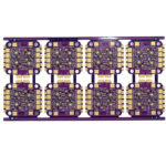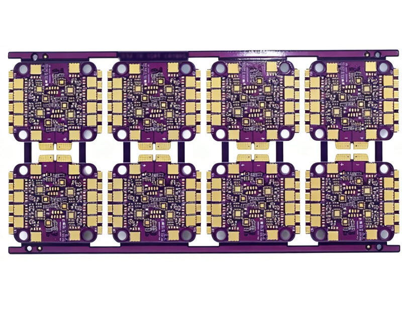
Multilayer PCB Inspection: Methods and Trade-offs
Multilayer PCB inspection is what separates a multilayer board that works from one that fails after installation. As soon as a design uses three or more conductive layers with insulating material between them, the defects that matter most are the ones nobody can see, and the test strategy has to be chosen with that in mind rather than inherited from a two-layer process.
Why multilayer boards are harder to check
A multilayer board is a stack of conductive layers separated by dielectric, built from base material such as FR4, conductive foil, insulating layers, and the interconnections that join them. The structure allows far more routing in the same area and much better electrical performance than a single-sided or double-sided board, which is why it dominates communications equipment, computer hardware, automotive control units, and medical devices.
The manufacturing sequence includes design, lamination, drilling, imaging, metallisation, and test, and each step demands its own quality control. The difficulty for inspection is that after lamination, the inner layers are sealed inside the stack. A defect created at imaging or plating is invisible from the surface, and it can be a short between two nets or an open that no surface measurement will reveal.
Visual inspection
The oldest method is still used, normally as a first pass. An operator examines the board under a microscope and looks for obvious problems: poor solder joints, misplaced components, or broken conductors. It suits low-complexity and small-batch work, where the cost of automated equipment cannot be justified.
Its limits are equally clear. The work is labour intensive, it depends on the attention of the operator, and it cannot see inside the stack at all. Visual inspection is a filter, not a test.
Automated optical inspection
Automated optical inspection uses high-resolution cameras to scan the board surface and pattern recognition algorithms to compare what they see against the expected image. It reliably finds surface defects such as poor solder joints, component misalignment, and pad problems, and it does so without contact and at production speed, which is why it is the standard method for high-volume assembly.
What it cannot do is see through copper. For a multilayer board, AOI provides real-time monitoring of the outer layers during manufacturing and nothing more, so an inspection plan built only on AOI leaves the inner layers untested.
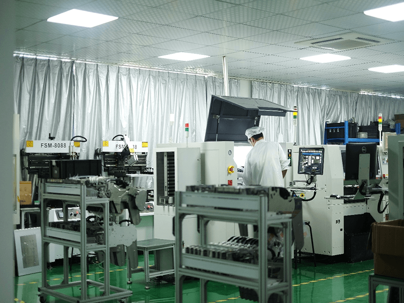
AOI finds what the camera can reach. A perfect optical result on a multilayer board means the outer layers are good, not that the board is good.
X-ray inspection
X-ray inspection sees through the stack. Because X-rays penetrate multiple layers, the method suits hidden defects: failed vias, internal shorts, and layer-to-layer soldering problems. It is the primary tool for high-density multilayer boards and for assemblies whose joints sit underneath a package, and it is often the only technique that can confirm a plated barrel is continuous.
The cost is time and money. X-ray systems are slower than optical systems and more expensive to buy and run, so they are applied where the alternative is an untested risk rather than as a routine step on every board.
Laser scanning inspection
Laser scanning sweeps the board surface with a laser and analyses the reflected light. It resolves very small surface defects such as micro-cracks and blisters, which makes it useful for a defined quality question. Its application is narrower than AOI, and it is normally deployed to solve a specific problem rather than as a general inspection stage.
Electrical test
Electrical testing applies current or voltage to the board and measures the result. Bed-of-nails fixtures and flying probe systems are the two common approaches. Both verify connectivity, conductivity, and isolation between nets, and they catch the opens and shorts that optical methods cannot see because those defects are inside the stack.
The limitation is scope. Electrical test proves that the netlist has been realised; it does not prove that the board is mechanically sound. A cracked pad, a marginal plating thickness, or damage at the board edge can pass an electrical test and still fail in the field.
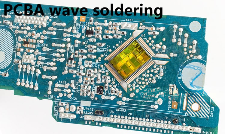
Test coverage and design intent have to be checked together. A net that cannot be probed is a net that will not be verified, no matter how capable the tester is.
Challenges specific to multilayer boards
Three problems recur. Inner-layer defects are hidden between outer layers, and because those inner layers often carry critical signals or power, one defect can compromise the whole board; X-ray inspection is the method that reveals internal opens and shorts. Via integrity is the second: vias are formed by plating, and a plating fault produces a connection that measures correctly when new and degrades under thermal cycling, so both optical and X-ray systems are used to confirm the barrel. The third is electrical integrity, which becomes harder to guarantee as layer count rises, because signal routing and power distribution grow more complex and problems such as noise, delay, and crosstalk can appear in a board with no visible defect at all.
Process control upstream reduces how much of this has to be found by test. Boards built with verified plating chemistry and a documented stackup fail differently than boards built without them, which is why copper plating defect prevention belongs in the same conversation as inspection.
Choosing the right method
Layer count sets the floor. For low layer counts, visual inspection and AOI may be sufficient. For high layer counts, X-ray inspection and electrical test become mandatory rather than optional, because the defects that matter can no longer be reached from the surface.
Cost, accuracy, and cycle time then decide the mix. AOI is inexpensive per board and fast, which suits volume production. X-ray delivers detail that nothing else provides but costs more per board and slows the line, so it is applied where the design demands it. Each method also has a blind spot. Visual inspection is simple and intuitive but labour intensive and prone to human error. AOI is fast and automated but blind to internal layers. X-ray resolves internal structure but is slower and more expensive. Laser scanning resolves minute surface defects but is not widely deployed. Electrical test validates the netlist but ignores mechanical defects.
Defects, escapes, and the cost of both
The defects worth designing around are three. A short connects two nets that should be separate and causes functional failure. An open breaks continuity so the signal never arrives. A cold joint forms a connection that is mechanically and electrically weak, so the product works until the joint is stressed.
A defect that escapes inspection reaches the customer, where the consequences run from a field failure to a safety hazard, and the cost of an escape always exceeds the cost of the inspection that would have caught it. Inspection that finds problems early in the process reduces rework and scrap, which lowers total production cost even though the test step itself adds time. The inspection strategy also shapes the prototype phase, since the requirements that will be verified later are the requirements that should be specified when the board is ordered; our guide to multilayer prototype requirements covers that handover. Where inner-layer access is the limiting factor, the stackup choices described in blind and buried via stack selection decide how much of the board remains reachable.
FAQ
Can AOI replace electrical test? No. AOI verifies appearance and placement, while electrical test verifies the netlist. A board can look perfect and still have an open inside the stack.
How much X-ray inspection is enough? Enough to cover the features that cannot be verified any other way, such as plated vias and joints beneath a package. Sampling is a risk decision, not a technical one.
Does inspection slow production too much? Only when the method is mismatched to the board. AOI on outer layers and electrical test on the netlist run at production speed; X-ray is reserved for the features where it is the only option.