PCB Gold Fingers: Plating Stack, Bevel and Wear Life
PCB gold fingers are the plated strips along a board edge that slide into a socket and carry power and signals between the board and the system. They look simple, and that is why they are often specified carelessly. The plating stack, the bevel, the finger geometry and the way the fingers are routed all determine whether the connector survives a thousand insertions or wears through in the first month.
This article covers what the gold layer is actually doing, how the plating stack is built, and the layout rules that keep an edge connector reliable.
What Gold Fingers Are and Why Gold
An edge connector is a set of exposed pads on the board edge, arranged on one or both sides of the board. The mating socket presses spring contacts against them, so the pads must resist wear, oxidation and the small amount of arcing that accompanies hot plugging. Gold does all three: it does not form a resistive oxide film, its contact resistance stays low at light loads, and it wears gradually rather than galling.
Gold is also the only common contact material that remains solderable and wire-bondable while staying stable in storage. That combination is why PCB gold fingers appear on memory modules, expansion cards, industrial backplanes and handheld instrument interfaces, even though the plating is one of the more expensive finishing options available.
Hard Gold Versus Immersion Gold
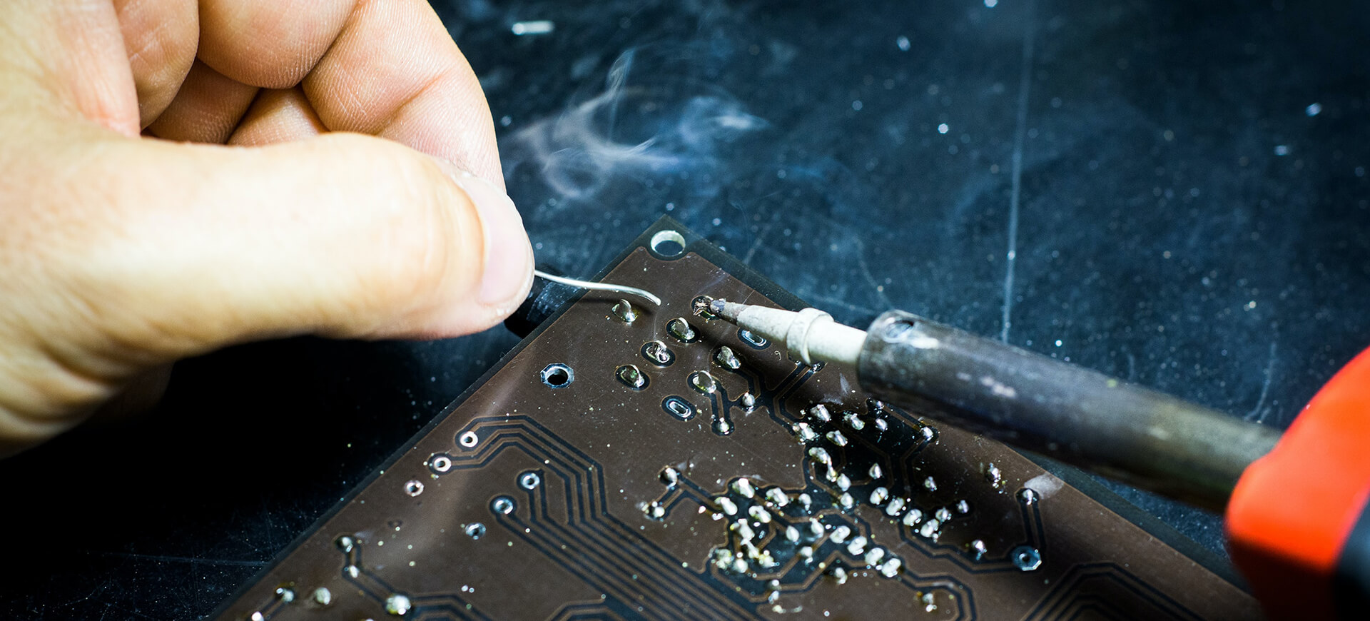
Gold over nickel, applied by electroplating, is called hard gold because the deposit contains a small amount of cobalt or nickel that raises its hardness. It is the correct choice for PCB gold fingers, because the contact will be inserted and removed many times and a soft deposit would smear and wear through quickly.
Immersion gold, by contrast, is a very thin chemical deposit used for soldering and for fine-pitch pads. It has no measurable wear resistance, so it should never be specified on a mating surface. Confusing the two is a common and expensive mistake, because the two finishes look identical on an incoming inspection bench.
The Nickel Underlayer Does the Work
Hard gold is always plated over nickel, and the nickel is what actually carries the mechanical load. A typical stack is 3 to 5 microns of nickel with 0.5 to 1.5 microns of hard gold on top. The nickel provides a hard, corrosion-resistant base that stops the gold from diffusing into the copper beneath it and gives the contact a defined contact geometry.
If the nickel is too thin, the gold deforms into the copper and the contact resistance rises as the surface roughens. If the gold is too thin, the nickel is exposed once the thin gold wears, and nickel oxide is a poor conductor. The plating quality rules that apply to barrel plating apply here as well: uniform thickness matters more than the nominal figure on the drawing.
<img src="https://www.gopcba.com/wp-content/uploads/2026/06/AI-Hardware-Manufacturing.jpg" alt="Bevel angle on gold plated edge contacts” />
Bevel and Chamfer
The leading edge of the finger area is machined to a bevel so the board slides into the socket without catching. A typical bevel angle is 20 to 30 degrees from the board surface, cut so that the fingers are not damaged and the socket contacts are not lifted as the board enters.
The bevel has to be applied after plating, and it exposes bare laminate and copper at the board edge if it is cut too deep. The rule is to keep the bevel within the non-functional area between the board edge and the start of the contact zone, and to ensure the socket contact never rests on beveled material. The board outline and mounting rules cover how that keep-out interacts with the rest of the mechanical design.
Layout Rules Around the Fingers
Finger width and pitch usually follow the socket rather than the designer’s preference, so the layout freedom is in what happens behind them. Every finger should be routed from its contact area with a short, direct stub, and the traces leading away should fan out gradually rather than turning immediately at the contact pad.
Ground and power fingers must be wider than signal fingers, and it helps to place them at the ends of the row where the socket contacts are mechanically most stable. Where several ground fingers exist, connecting them to an internal plane close to the contact area gives the return current a short path and reduces the inductive drop that appears on the supply during a hot-plug event. Standard pad design rules apply to the finger dimensions once the socket tolerance has been taken into account.
Wear Life and Insertion Cycles
Contact life is quoted in insertion cycles, and the figure depends on the plating thickness, the contact force and the environment. A well-built edge connector with 1 micron of hard gold over nickel typically survives tens of thousands of cycles in a clean, dry environment, and a much smaller number where the contacts are exposed to dust, salt spray or repeated temperature cycling.
Two practical measures extend the life. The first is to avoid hot plugging wherever possible, because the arc that forms as the contacts separate erodes the gold and exposes the nickel. The second is to keep abrasives away from the contact zone, which in practice means covering the fingers with tape during assembly and cleaning if the board will be handled repeatedly before it is fitted.
Contact force is the third variable, and it belongs to the socket rather than to the board. A socket with light contact force wears the gold more slowly but is more susceptible to intermittent contact when the surface is contaminated, while a heavy contact force keeps the resistance stable but wears through the plating sooner. Matching the plating thickness to the socket specification is the only way to predict the life of the pair.
Cost and Substitutes
Hard gold plating is expensive, so it should be applied only where it is needed. A common approach is selective plating: the finger area receives the full nickel and hard gold stack, while the rest of the board receives a cheaper finish. This requires the fabricator to mask the board in two stages and adds a handling step, but the material saving usually outweighs it.
Where the connector will be mated only a few times, a tin finish or a thin gold flash over nickel may be adequate, though both have drawbacks. Tin forms an oxide and requires a wiping contact to break through it, while a thin flash wears through quickly. Neither is a substitute for hard gold on a surface that will be inserted repeatedly.
FAQ
How thick should hard gold be for PCB gold fingers? Between 0.5 and 1.5 microns over 3 to 5 microns of nickel covers most applications. Thicker gold improves wear life only marginally, because the wear rate is governed by the contact force and the environment rather than by the reserve of gold.
Can gold fingers be soldered? They can, but they should not be. Solder wicks along the gold and can bridge adjacent fingers, and the resulting alloy is brittle. Fingers are designed to be mated, and any component that needs soldering belongs elsewhere on the board.
Why do my fingers turn dark in storage? Darkening usually indicates porosity in the gold, which lets the nickel beneath oxidise, or contamination from handling. Both are process issues, and the answer is usually a thicker gold deposit and clean gloves during inspection.