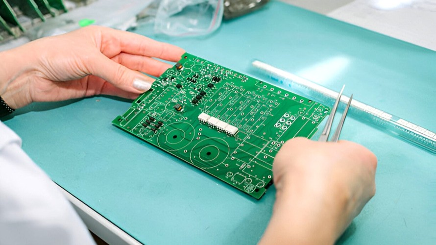
Double-Sided PCB Manufacturing: Process and Design Rules
A double-sided PCB carries copper on both surfaces and connects the two with plated through-holes. It is the workhorse of electronic manufacturing: more capable than a single-sided board, far less expensive than a multilayer stack, and adequate for the majority of products that do not need controlled impedance or high routing density.
Manufacturing it involves a plating process that a single-sided board never sees, and that single step is what makes the design rules different.
What a Double-Sided Board Provides
The two copper layers can cross each other, because a connection between them is made through a plated hole rather than on the surface. Routing that would require a jumper on a single-sided board becomes a short via, which removes a component and an assembly step at the same time.
A double-sided board also allows a ground or power area on one side while signals route on the other. That arrangement lowers noise compared with a single-layer design, because return currents have a defined path rather than spreading through the panel.
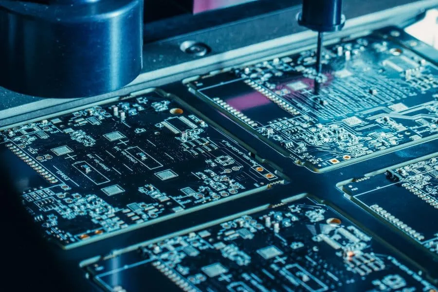
Step One: Drilling
Holes are drilled before plating, in a numerically controlled machine that reads the drill file directly. Hole size, position and the condition of the hole wall all determine whether the plating step can make a reliable connection.
Design rules follow from this. Hole size should be generous enough for the plating process, position tolerance must be accounted for in the pad size, and the number of distinct hole sizes should be kept low, because every tool change adds cycle time to the drilling operation.
Step Two: Through-Hole Plating
Plating makes the hole walls conductive. A thin electroless copper layer is deposited chemically, then electroplating thickens it to the specified wall thickness. The same plating step adds copper to the surface of the board.
Because copper is added rather than only removed, outer layer traces are usually defined by a pattern plating process in which the plating resist protects the traces and the plating current is distributed across the panel. Plating uniformity depends on the copper distribution, which is why designs with large isolated areas of copper may need current thieves or a balanced pattern.
<img src="https://www.gopcba.com/wp-content/uploads/2026/08/pcb2.jpg" alt="Double-sided panel during solder mask and plating stages” />
Step Three: Imaging and Etching
After plating, the outer layers are imaged and etched. Etch factor affects trace width in the same way it does on a single-sided board, but the starting copper is thicker because of the plating, so the trapezoidal cross section is more pronounced.
Design rules for trace width on a double-sided board therefore need margin. Working at the process minimum for width and gap leaves no room for the etch spread, and the most common yield loss on this class of board is a short between closely spaced traces.
Step Four: Solder Mask and Legend
Solder mask is applied over the whole panel and then imaged so that pads, test points and connector fingers remain exposed. Registration between the mask and the copper determines how much mask remains on the pad edges and how wide the dams between fine-pitch pads are.
On a double-sided board, mask registration matters on both sides. A mask opening that is consistently offset on one side indicates a tooling problem, and the resulting exposure of copper near a pad can produce solder bridging during assembly.
Step Five: Surface Finish
Surface finish protects the exposed copper. Hot air solder levelling is the traditional choice for double-sided boards because it is inexpensive and durable, and it handles the coarse pitch typical of this board class. Immersion silver and electroless nickel immersion gold are used where finer pitch or longer shelf life is needed.
The finish must suit the assembly process. A finish that oxidizes during storage produces wetting defects, which appear as incomplete fillets on through-hole joints and as intermittent opens on surface-mount pads.
Step Six: Electrical Test and Routing
Finished boards are electrically tested for continuity and isolation using a fixture built from the netlist. Test points should be designed in, because probe access on a dense double-sided board is limited and adding test points to the fixture after layout is not possible.
Boards are then routed out of the panel. Panel size, rail width and the number of boards per panel affect the handling cost per unit, and a small change in board dimensions can change the number of boards that fit a standard panel.
Design Rules for Double-Sided Boards
Keep the copper balanced between the two sides. A board with a large ground pour on one side and sparse routing on the other tends to bow during lamination and again during reflow, and a bowed board cannot be placed reliably.
Size pads for the drill tolerance plus registration. Annular rings that are comfortable at nominal values become marginal after drilling and plating, and a marginal ring is a reliability risk rather than an immediate defect.
Where the design allows, put the ground on one side and the signals on the other. This gives every signal a return path directly beneath it and reduces the loop area that radiates and receives noise.
Panelization and Manufacturability
Panelization is part of the design rather than the fabricator’s convenience. Rails wide enough for conveyor handling, tooling holes, fiducials on every panel and a break-away method that does not stress components all reduce assembly problems later.
The break-away method matters more than it appears. V-cut is fast but leaves a rigid edge and stresses the board during separation, while routed tabs with perforations allow cleaner separation on assemblies with components close to the edge.
Cost Structure
Cost is dominated by area, layer count, hole count and finish. Drilling and plating are the steps that separate a double-sided board from a single-sided one, and their cost scales with the number of holes rather than with the area.
Reducing the number of distinct hole sizes, keeping the board within a standard panel size and avoiding unnecessary finish upgrades do more for cost than any other design change on this class of board.
When to Move to Multilayer
A double-sided board stops being the right choice when routing congestion forces long detours, when a fast interface needs a continuous reference plane, or when electromagnetic compatibility requirements cannot be met without a ground plane.
Those conditions usually arrive together. Once a design needs a controlled impedance line or a dense ball grid array, the four-layer board becomes cheaper than the engineering effort required to make two layers work.
Related reading: via design rules, trace width and current calculation, and board outline and mounting design.
FAQ
Is a double-sided board suitable for high-speed signals? For moderate speeds with a ground plane on the opposite side, yes. Once rise times are short and impedance must be controlled, a multilayer stack with an adjacent reference plane is required.
How does hole count affect price? Drilling and plating both scale with holes, so a design with many small vias costs more than one with fewer, larger holes. Reducing the number of distinct hole sizes also reduces machine time.
What is the most common double-sided design mistake? Working at the minimum trace and gap. The etch and plating processes produce a spread around the nominal value, and a design with no margin fails as shorts rather than as opens.