Direct Bonded Copper PCB: Differences from Standard Materials
Direct bonded copper sits at the high end of thermal substrate technology. It joins thick copper to a ceramic base at high temperature, producing a conductor that carries hundreds of amps and spreads heat across the ceramic at the same time, which is why it dominates power modules and traction inverters.
What Direct Bonded Copper Is
The process bonds a copper sheet to a ceramic tile under heat and pressure in an atmosphere that prevents oxidation. At the bonding temperature a thin copper-oxygen eutectic forms at the interface and creates a bond strong enough to survive thermal cycling without an adhesive layer.
Conductors are then etched from the copper in the usual way, leaving a pattern with a thickness that organic laminates cannot match. The result is a substrate that is simultaneously the insulator, the conductor and part of the heat path.
How It Differs from FR-4 and Metal Core Boards
An FR-4 board carries current in thin copper and conducts heat poorly, relying on thermal vias and copper area to move energy away from a hot device. A metal core board improves on that with an aluminium base and a thin insulating dielectric, but the dielectric is the limiting layer and the base is conductive.
A direct bonded copper substrate replaces both. The ceramic is a true insulator with thermal conductivity many times that of FR-4, and the copper can be hundreds of microns thick. Where a power device must be isolated from a heat sink and still dissipate hundreds of watts, that combination is the reason the technology exists.

Copper Thickness and Current Capacity
Standard DBC substrates use copper between roughly 0.1 and 0.6 mm thick, which is an order of magnitude above typical laminate foil. Resistance falls in proportion, so a modest width carries a large current with little loss, and the copper also acts as a lateral heat spreader that distributes the device’s heat across a much larger ceramic area.
Thicker copper is not automatically better. A thicker layer requires a longer etch and holds a wider minimum feature, and the increased stored strain energy at the copper-ceramic interface makes the substrate more prone to cracking during thermal cycling.
Thermal Resistance Path
The thermal path from a semiconductor junction runs through the die attach, the copper, the ceramic, the second copper layer and the interface to the heat sink. Each element contributes resistance, and the ceramic is usually the largest single term.
Material choice therefore has a direct effect. Alumina provides a good balance of cost and performance, while aluminium nitride roughly doubles the thermal conductivity at a higher cost. The selection is made by calculating the junction temperature for the worst-case ambient, and the result usually determines whether the design is feasible at all.
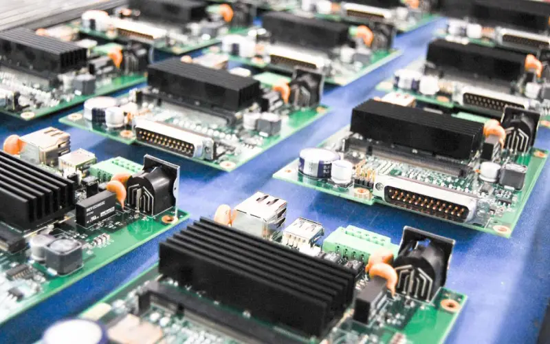
<img src="https://www.gopcba.com/wp-content/uploads/2025/08/12温区氮气回流焊.jpg" alt="Power module mounted on a direct bonded copper substrate” />
Pattern Limits and Mechanical Rules
The copper pattern is constrained by the stresses the bond can tolerate. Large unbonded areas create local ceramic stress, so the design rules limit the size of isolated copper regions, the width of copper-free channels and the spacing between copper features.
Corners are rounded and internal angles are kept obtuse where possible. Where a large copper area is unavoidable, it is often subdivided by narrow channels that relieve stress without interrupting the current path significantly.
Applications in Power and Automotive Electronics
Traction inverters, on-board chargers, photovoltaic converters, motor drives and high-power LED modules are the familiar users. In each case the requirement is the same: a large current, a high ambient temperature and an isolation barrier that must hold for the life of the product.
Automotive qualification adds thermal cycling and power cycling requirements that test the bond line rather than the device. A substrate that passes an initial test can still fail after thousands of cycles if the copper pattern concentrates stress at a corner, which is why the pattern rules matter as much as the material specification.
Assembly and Attachment
Devices attach by soldering, by sintering silver or by wire bonding, depending on the power level and the temperature limits. Sintering produces a joint with excellent thermal and electrical performance, but it requires pressure and temperature during assembly and is less forgiving of surface condition.
The substrate is then mounted to a heat sink with a thermal interface material and a mechanical clamp. Uneven clamping pressure is a common cause of premature failure, because the ceramic is strong in compression and weak in bending.
Comparison With Other Thermal Substrates
A direct bonded copper substrate also needs a different fabrication partner than a laminate board, since the ceramic bonding and thick copper etching are specialised processes. For moderate power, a metal core board or an FR-4 board with a dense thermal via array is adequate and far cheaper. For very high power density with a strict isolation requirement, direct bonded copper is usually the only practical option, and the general conventions for such builds follow fabrication practice.
The decision should be quantitative. Estimating the junction temperature for each candidate and comparing the cost of the resulting assembly is more reliable than choosing by category, and reviewing trace width and current calculations for the conductor thickness involved keeps the electrical side consistent with the thermal choice.
Designing for Repairability and Test
A DBC assembly is not easily reworked, so the design should minimise the need. Where a device may have to be replaced, the process should be defined in advance: heating the whole substrate, protecting the bond line and controlling the cooling rate to avoid cracking.
Test access is also limited because the copper is often covered by a solder mask or a coating. Planning probe points before the pattern is released avoids a situation where production testing requires special contacts. Reviewing board outline and mounting design alongside the thermal stack keeps the mechanical and electrical constraints aligned.
Quality Control for Direct Bonded Copper
The bond line is invisible in the finished part, so quality control relies on destructive and non-destructive sampling. Ultrasound inspection can reveal voids and delamination at the copper-ceramic interface without cutting the substrate, and it is normally applied to a sample from each batch.
Thermal cycling on a sample is the second check. Cycling between temperature extremes and then inspecting for cracking at pattern corners tests the specific failure mode that this technology is prone to, and it validates both the material and the pattern design together.
Copper thickness and pattern dimensions are verified separately, since they determine the electrical performance. A substrate that passes the mechanical tests but has copper thinner than specified will still overheat, and the two characteristics need independent acceptance criteria in the specification.
FAQ
Is DBC the same as a ceramic PCB? A DBC substrate is a ceramic board with thick bonded copper. Ceramic substrates can also be metallised by thick film or thin film processes, which suit lower currents and finer features.
Why does a DBC substrate crack in thermal cycling? The copper and ceramic expand at different rates, and the stored strain concentrates at pattern edges and corners. Following the pattern design rules and keeping copper areas modest is the standard prevention.
Can DBC replace a metal core board in LED products? For high-power assemblies with strict isolation requirements, it often does. For ordinary lighting, a metal core board usually provides adequate performance at much lower cost.