
PCB Manufacturing Defects: Causes and Prevention
Every fabrication process has failure modes, and the useful thing about PCB manufacturing defects is that almost all of them are predictable. They cluster around a small number of physical mechanisms, they are visible under the right inspection, and they respond to specific process controls. Knowing which defect belongs to which mechanism makes it possible to fix the cause instead of screening the symptom, which is the difference between a stable process and a permanent rework station.
Short and Open Circuits
An unintended copper connection between two nets is a short, and a broken connection is an open. Shorts usually come from incomplete etching, from resist that did not develop cleanly, or from conductive debris that survived the final rinse. Opens come from over-etching, from a scratch in the resist before etching, or from a fine trace that was damaged during handling after the copper pattern was defined.
Both mechanisms respond to the same control: etch rate and conveyor speed must be matched to the copper thickness and the pattern density. A panel with both very fine and very heavy copper areas will etch unevenly unless the process compensates, which is why design decisions that reduce that contrast also reduce defects. The interaction between plating and etching on the same panel is described in copper plating defects prevention.
Plating Voids and Thin Barrel Walls
A plating void is a gap in the copper that lines a drilled hole. Visually the hole may look normal, but the electrical connection is weak and the failure appears later as an intermittent open after thermal cycling. Causes include an aspect ratio that is too high for the chemistry to throw into, contaminated or out of balance bath, and insufficient current density or agitation during plating.
Prevention is a matter of keeping all three under control. Aspects ratios should stay inside the fabricator’s qualified range, bath chemistry should be analysed on a schedule rather than when a defect appears, and plating thickness should be monitored from coupons on every panel rather than from a sample. Back drilling and via filling add further constraints and warrant the same monitoring.
Delamination and Measling
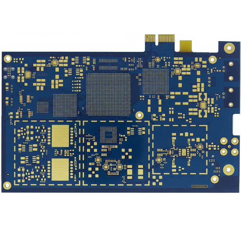
Delamination is a separation between layers, and it usually originates in moisture. Laminate absorbs water from the air, and when the panel is heated during lamination or reflow that water turns to steam and pushes the layers apart. The result may be a visible blister, or it may be an internal separation that only shows up in cross section or after thermal stress testing.
Baking before lamination and controlled storage are the standard countermeasures, and incoming material should be checked for its moisture state rather than assumed dry. Material compatibility matters as well: prepreg and core from different sources may have different resin flow characteristics, and a stackup built from mismatched materials can delaminate even when every individual material is within specification.
Solder Bridges and Pad Defects
A solder bridge connects two adjacent pads or leads that should be separate. In assembly the usual causes are excess paste volume, a stencil aperture that is too large for the pitch, poor paste release that leaves paste smeared between apertures, or a reflow profile that does not allow the paste to pull back onto the pad. Fine pitch parts and connectors with narrow spacing are the most exposed.
Pad lift is a different mechanism with an assembly origin. A pad separates from the laminate when it is overheated during soldering or when mechanical stress is applied while de-panelling, particularly where the board was routed or scored close to a pad. Reducing soldering temperature, using a proper depanelling method and keeping routing away from component pads all reduce the incidence.
Defects With a Design Origin
Some defects are designed in rather than manufactured in. An annular ring that is too small for the drilling tolerance produces a breakout. A trace that is narrower than the process can etch reliably produces intermittent opens. Copper that is unbalanced across a panel encourages warp, which then causes handling damage and assembly problems.
Those issues are exactly what a PCB design quality review is meant to catch, and they are cheaper to fix in the file than in production. Where a defect recurs across builds of the same design, the cause is usually in the design rules rather than on the line, and changing the process will not fix it.
Inspection Methods and What Each Catches
Visual inspection catches surface problems such as bridging, contamination and obvious damage. Automated optical inspection compares the copper pattern or the assembled board against the design data and catches the classes of defect that a human eye misses at speed. X-ray inspection reveals what cannot be seen optically, including voids in plated barrels and insufficient solder under area array packages.
Electrical test then verifies connectivity and, where required, impedance. The useful discipline is to decide which defects each stage is responsible for catching and to measure the escape rate, because an inspection step that finds nothing may either be redundant or be set too loosely. Coupon based testing of plating thickness and dielectric parameters adds physical evidence that the process, not just the product, is under control.
Prevention Through Process Control
The durable answer to defects is a controlled process with statistical monitoring. Key parameters such as etchant concentration, plating current density, lamination temperature profile and reflow peak temperature should be recorded per run and reviewed for drift, so that a trend is corrected before it produces scrap. Process control also covers equipment condition, because a worn drill or a contaminated stencil produces the same defect as a wrong parameter.
Material control completes the picture. Incoming laminate, prepreg and solder mask should be verified against the datasheet, stored under the conditions the manufacturer specifies, and traceable to the boards that used them. A partner such as gopcb records those parameters against each build, which turns a defect investigation from a guess into a comparison between a good run and a bad one.
What Defects Cost and How to Close the Loop
The cost of a defect depends on when it is found. A short caught during electrical test costs the price of the board. The same short caught after assembly costs the board, the components and the assembly time, and one that escapes to the field costs the return, the diagnosis and a share of the customer’s confidence. That progression is why inspection is placed as early in the flow as it can reliably catch the class of defect it targets.
Closing the loop matters more than the inspection itself. Every defect should be recorded with its location, its class and the process parameters of the run that produced it, and the data should be reviewed on a schedule rather than only when a customer complains. A Pareto of defect classes by process step usually shows that one or two steps account for most of the loss, and correcting those is far more productive than tightening inspection everywhere.
FAQ
What is the most common PCB manufacturing defect? Shorts and opens caused by etching variation, followed by plating quality issues in small drilled holes. Both trace back to process parameters rather than to a single bad panel.
Why does delamination happen after assembly? Because moisture absorbed into the laminate turns to steam during heating. Baking before lamination and controlled storage remove most of the risk.
Can a plating void be seen without X-ray? Not reliably. A void inside a plated barrel is invisible from the surface, which is why cross sections and electrical test on coupons are used to monitor plating quality.