Practical Notes on Embedded Copper Coin
Power density keeps rising in electric vehicle controllers, AI accelerator cards, industrial inverters and telecom power amplifiers, and the weakest link in those designs is often the path heat takes out of the die. An embedded copper coin PCB attacks that problem at the source by placing a solid copper block directly beneath the device, so heat reaches the heatsink through metal instead of through laminate and a field of vias. The result is a lower junction temperature and a longer service life.
What an Embedded Copper Coin Is
An embedded copper coin is a machined piece of pure copper pressed into the laminated structure of the board, positioned under a high dissipation component such as a MOSFET, IGBT, CPU or GPU. Unlike a thermal via array that carries heat layer by layer through plated barrels, the coin forms a continuous low resistance channel from the component pad to the opposite side of the board, where it meets the heatsink or the metal housing.
Typical coin thicknesses are 0.5 mm, 1.0 mm, 1.5 mm, 2.0 mm and 3.0 mm, with custom parts available beyond 8 mm. The material is usually C1100 or oxygen free high conductivity copper with a thermal conductivity near 390 to 400 W/mK, compared with roughly 0.3 W/mK for FR-4 and about 170 W/mK for an aluminum substrate. That gap is the entire reason the technology exists, and it also explains why the coin can carry current as well as heat. Designing the surrounding copper for that current is covered in trace width current calculation.
Why Copper Changes the Thermal Path
Heat leaving a power device crosses several interfaces before it reaches ambient air, and each one adds thermal resistance. A conventional design routes that heat through a thermal via field into inner copper planes and then to the far side, which works well for moderate loads but saturates once current and switching losses rise. Spreading heat laterally through thin copper also raises the temperature of neighboring components, which is rarely acceptable.
A copper coin shortens the path dramatically and lowers thermal resistance at the same time. Because the coin is a bulk conductor rather than a plated barrel, it handles both the heat flux and the current of the power stage, so designers frequently use it as the drain or source connection as well. The mechanical benefit matters too: a thick copper insert stiffens the local area, which reduces warpage when the board sees reflow temperatures and repeated thermal cycling. The return current around the coin also has to be handled deliberately, as described in ground routing and power trace planning.
Pocket Milling and Coin Insertion
The process starts with the copper itself. The coin is machined on CNC equipment to tolerances around plus or minus 0.02 mm, and flatness, surface roughness and dimensional consistency all have to be held, because any error propagates into the laminated panel. The core is then milled with a matching pocket, and that pocket must be free of burrs with smooth walls and enough clearance for resin to flow around the insert.
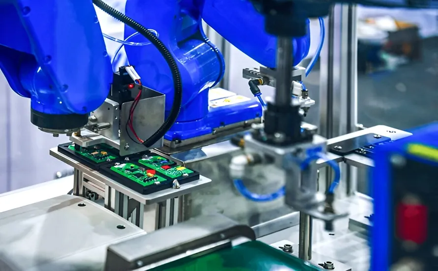
Placement comes next. The coin is positioned in the pocket with alignment error held to roughly 30 microns, and the surrounding prepreg is built to fill the gap without voids. Resin flow is the critical variable: too little and voids form beside the coin, too much and the dielectric thickness collapses. On thicker boards several coins may be set into one panel, and each pocket depth has to be controlled so the finished stackup stays flat.
Vacuum Lamination and Planarity
The panel then goes into a vacuum press, where heat, pressure and vacuum together consolidate the coin and the laminate into a single structure. Vacuum lamination is essential rather than optional here, because trapped air beside a large copper block cannot escape through a solid metal wall. After pressing, the panel is ground to bring the coin flush with the surface and to restore flatness, usually within about 30 microns so that BGA and QFN packages can be placed reliably.
Copper deposition and plating follow, first electroless copper and then electroplated and pattern copper, which ties the coin into the conductive layers around it. Surface finish is selected from ENIG, immersion silver, immersion tin, OSP or hard gold according to the assembly process. Inspection then covers automated optical inspection, X-ray, flying probe, hipot, thermal resistance measurement, dimensional checks and warpage, and any of those can catch a coin that shifted during pressing.
Design Rules That Prevent Failures
Copper coin designs fail for predictable reasons, and most of them are decided at the layout stage. Keep the coin area no larger than necessary so that lamination stress and resin starvation stay manageable, balance copper across the board to control warp, and provide enough resin flow channel around the coin so it fills completely. Clearance between the coin and any signal layer has to satisfy the working voltage, with a defined creepage distance on high voltage rails. Where the plating and the coin meet, defect control follows the same rules as copper plating defects prevention, since voids and thin copper at that junction become hot spots later.
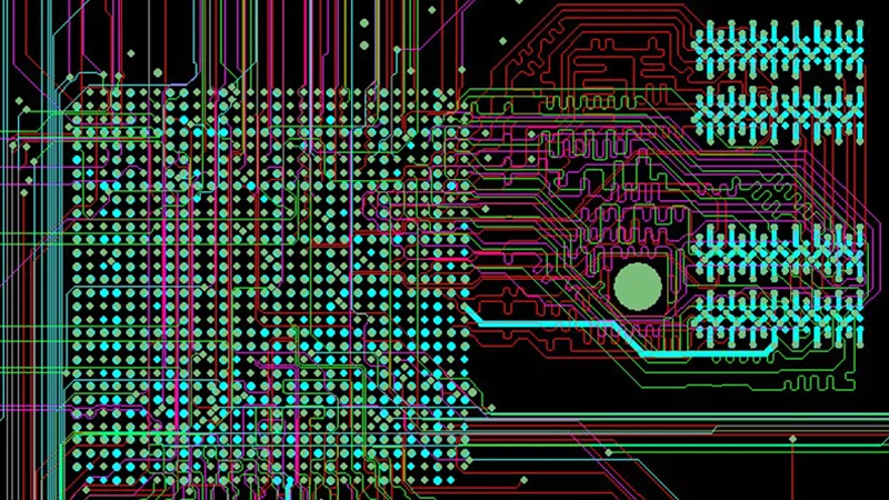
Thermal expansion mismatch deserves early attention because copper, FR-4 and ceramic materials move at different rates. The coin should be considered in the stackup from the beginning, with the dielectric thickness above it specified so that impedance and drill depth behave as expected; the same reasoning applies to any high layer count build described in PCB dimensional stability. Finally, plan for flatness, because the combined tolerance of the coin, the pressed laminate and the grinding step has to stay inside the placement budget of the package being mounted.
Two more rules save expensive rework. Never place the coin so that it creates an isolated copper island on an inner layer, since that both unbalances the press and complicates plating. And always confirm that the thermal path continues after assembly, which means the opposite side of the board needs a flat, well coupled interface to the heatsink rather than a thin solder mask layer over bare copper.
Cost and Application Fit
Copper coin boards sit in the middle of the cost and difficulty scale. A thermal via field is cheap and easy to make but limited in capacity. A heavy copper PCB and an insulated metal substrate board cool better, yet neither offers a direct metal path from die to heatsink. Ceramic substrates outperform everything thermally at a much higher price. An embedded coin costs more than a thick copper board but usually less than ceramic, which is why it appears in cost sensitive high power products.
Applications follow the same logic: motor controllers, on board chargers, DC/DC converters and battery management in electric vehicles; GPU and accelerator cards in AI servers; inverters, servo drives and welding equipment in industrial power; photovoltaic inverters and energy storage; and 5G base stations, high power amplifiers and radar modules. In all of these the coin is what allows the device to run at full rating without derating.
Pricing depends on layer count, coin size, material, process complexity and order quantity. Prototype builds typically run from around 180 to 450 USD for two layer work and 400 to 900 USD for four to eight layers, plus more for complex high layer count designs. Small batches of 50 to 500 pieces usually fall near 40 to 150 USD each, while volumes above a thousand pieces come down to roughly 8 to 60 USD, with CNC pocket milling, vacuum lamination, X-ray and thermal testing the main cost drivers.
FAQ
What is an embedded copper coin PCB? It is a board with a solid copper block laminated into the structure, positioned under a high power component so heat flows through metal to the heatsink instead of through the dielectric and a via field.
Is a copper coin better than a thermal via array? For high power devices, yes. The coin offers a shorter path and lower thermal resistance, and it can carry current as well as heat, which a via field cannot do as efficiently.
How thick can the coin be? Common sizes run from 0.5 mm to 8 mm, and custom parts beyond that are possible when the stackup and the press cycle are designed around them.
Can it be combined with HDI or thick copper? Yes. Copper coins are routinely combined with HDI, blind and buried vias, heavy copper layers and controlled impedance in the same stackup, and a fabrication partner such as gopcb will confirm the press window before release.