Edge Plating Requirements for PCB Fabrication
Edge plating is copper that wraps from the top side of a board around the cut edge to the bottom side. It is used for shielding continuity, for high current paths between layers, for soldering a board into a metal frame and for the castellated modules that are soldered onto a carrier.
The process looks like an extension of ordinary plating, and the difference is that the edge is machined after the copper is deposited. That order of operations creates requirements that do not exist anywhere else on the board, and it is why a design that specifies edge plating has to be discussed with the fabricator before the data is released.
What Edge Plating Is Used For
The most common use is shielding, where the edge copper connects the ground planes of several layers to a metal housing or to a gasket. The connection has to be continuous, so the plating has to be free of gaps and the copper on each layer has to reach the edge.
The second use is a module that is soldered onto a carrier by its edges, where the castellation carries both the electrical connection and the mechanical retention. The third is a high current path, where the edge carries more current than a trace of reasonable width could on the surface.
Design Data Requirements
The fabrication data must state which edges are plated, the copper thickness on the edge, the tolerance on the finished outline and the finish that will be applied to the edge. A drawing that simply says edge plating leaves the fabricator to assume all four.
The copper layers that reach the edge must be identified as well, because a plated edge that does not connect to any plane is decorative while one that connects to a plane is functional. The difference is not visible after the board is completed.
Copper Pull Back and the Edge Strip
Ordinarily the copper on each layer is pulled back from the board outline by a small distance so that the router does not cut through it and leave a burr. Edge plating requires the opposite, with copper brought to the edge and a continuous strip formed along the perimeter.
The strip has to be wide enough to survive the routing tolerance and to carry the current. On a typical design the copper extends to the outline and the layers that should be connected are tied together by a band that is at least a few tenths of a millimetre wide after processing.
Routing Sequence and Machining
The edge is machined after plating, so the copper that is exposed at the cut is the copper that was on the wall of the strip. The router has to cut cleanly, because a rough cut leaves a torn edge that cannot be plated over and that will not solder.
Where castellations are required, the holes are drilled before the edge is cut and the cut removes half of each hole. The remaining half barrel becomes the castellation, so the position of the cut relative to the hole is a tolerance that determines the shape of the finished feature.
Burrs and Edge Quality
A burr is a ridge of copper or laminate left by the cutting tool, and on an edge plated board it is a serious defect because it changes the outline and can interfere with a mating part. Burr removal adds a step and must be specified.
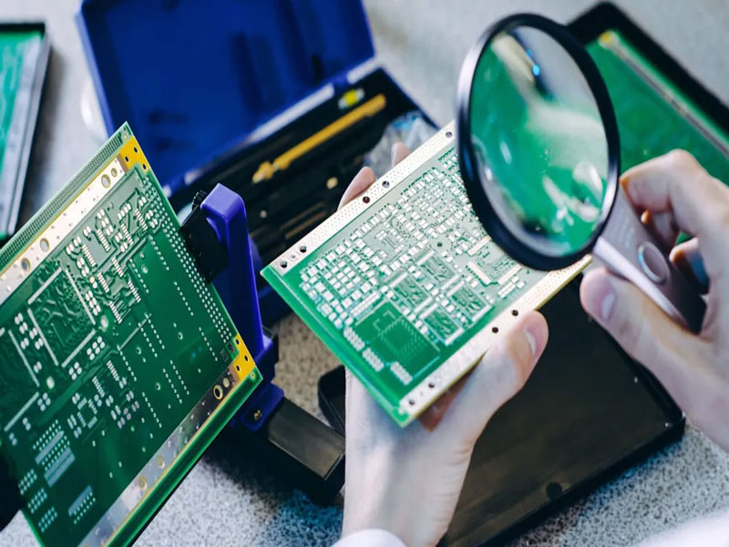
Deburring by hand on a fine outline risks damaging the plating, so the process is normally a controlled brush or a chemical deburr with a defined material removal. The finished edge should be inspected at magnification before the boards are shipped.
Solderability of the Plated Edge
Where the edge will be soldered, the surface finish has to cover the plated copper, and applying a finish to a vertical surface is harder than to a flat one. Immersion finishes follow the copper well, while a hot air levelled finish on an edge is uneven and difficult to control.
The finish choice should be made with the soldering method in mind. A module that is soldered by reflow benefits from a finish that wets readily, while an edge that merely contacts a gasket needs only corrosion protection, and the two requirements lead to different specifications.
Castellated Modules
A castellated module is a small board with half holes along its edges, soldered onto a carrier like a large component. The castellation provides the solder joint, and its quality depends on the plating thickness inside the half hole and on the flatness of the carrier.
The paste volume has to be calculated for a joint that is partly vertical, and the stencil aperture on the carrier is usually extended beyond the pad to allow for it. This is a case where the assembly and the fabrication requirements are set together, as they are for the pads described in pad design standards.
Thickness of the Plated Copper
The copper on the edge is deposited during the plating of the board, so its thickness follows the plating specification rather than being applied afterwards. A thicker edge requires a longer plating cycle and affects the whole board rather than the edge alone.
Where the edge carries current, the thickness should be chosen from the resistance requirement, and the calculation should account for the fact that the deposited copper fills the barrel as well as the surface. A current carrying edge is often the reason a board moves to a heavier copper weight overall.
Inspection and Acceptance
Inspection covers continuity around the perimeter, the absence of gaps between the copper and the laminate, the burr condition and the finish coverage. Continuity is checked electrically where the edge is part of a ground path, and visually elsewhere.
A cross section through the edge shows the copper thickness and the bond between the plating and the laminate. Where the edge is critical, the section should be taken from a coupon built with the panel, since a production board cannot be sectioned without being destroyed.
Cost and Lead Time Effects
Edge plating adds process steps, adds handling and reduces the number of boards that fit on a panel, so it should be specified only where it is needed. It is also one of the features that limits the choice of fabricator, because not every shop has the equipment to machine and plate an edge reliably.
The design should therefore distinguish between a plated edge that is functional and one that was specified for appearance, and the documentation should give the tolerance on the outline that the process can actually hold. Overspecifying an outline tolerance on a plated edge is a common cause of cost without benefit.
Related reading: our fabrication notes, board quality and design release notes cover the same ground.
A first article check confirms that the process and the drawing agree on the points listed above, and that the coupon data supports the values used in the design.

Where a measurement falls outside the expected window, the sample is retained so that the cause can be established before the balance of the batch is released.
A first article check confirms that the process and the drawing agree on the points listed above, and that the coupon data supports the values used in the design.

Where a measurement falls outside the expected window, the sample is retained so that the cause can be established before the balance of the batch is released.
FAQ
Can any board have edge plating? Most can, but the edge must be free of components and the layers that reach the edge must be defined, so the layout has to leave the perimeter clear.
Does edge plating replace a ground plane connection? It supplements it. The edge provides a low impedance path to a housing, while the planes still carry the return currents inside the board.
Is a castellation the same as edge plating? It is a form of it. The half hole is plated in the same operation, and the difference is the geometry of the finished feature rather than the process.
What finish is best for a soldered edge? A metallic immersion finish, because it covers a vertical surface evenly and wets predictably during reflow.