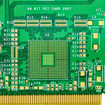
Hatch Plane Design On PCB Layers
A hatch plane is a copper area filled with a grid of lines rather than with solid copper. It carries the same net as a solid plane and it is connected the same way, but the material is removed in a regular pattern, which changes its electrical behaviour, its thermal behaviour and its effect on the lamination.
This article covers what a hatch plane does differently from a solid plane, how the pattern is dimensioned, and where each is appropriate.
What A Hatch Plane Is
The pattern is generated by the layout tool, usually as a grid of crossing lines with a defined trace width and a defined gap. The lines are connected to each other and to the net, so the plane is electrically continuous, and the open areas between them expose the laminate. The pattern is normally applied to a plane that is not a critical reference surface, and the parameters are chosen so that the hatch is much finer than any wavelength of interest in the design.
The reason for hatching is usually mechanical or thermal rather than electrical. It reduces the amount of copper bonded to the laminate, which changes how the resin flows during lamination, and it gives the laminate somewhere to expand into when the assembly is heated. Where the board has a large area of plane, that can be the difference between a flat board and a warped one.
Electrical Differences From A Solid Plane
A solid plane is the best reference for a transmission line, because it provides a continuous return path directly beneath the trace and a well defined capacitance per unit length. A hatch plane provides the same return path in principle, but the current has to flow around the openings, so the effective inductance of the return path rises and the impedance of a line above it becomes both higher and more variable.
Quantitatively, the difference is small when the hatch is fine compared with the distance to the trace and the frequencies are moderate, and it becomes significant when the pattern dimensions approach the distance to the reference or the wavelength. A fine hatch with a line width and gap of a few tenths of a millimetre under a trace at a distance of a tenth of a millimetre behaves almost like a solid plane; a coarse hatch under a high speed differential pair does not. The comparison of fill styles is treated under copper flooding: mesh or solid.

Thermal Behaviour
A hatch plane removes less heat from a pad than a solid plane, because the copper cross section available for conduction is smaller. That can be an advantage during soldering, where a solid plane makes a joint difficult to heat, and a disadvantage in service, where the plane is expected to carry heat away from a component or to spread it across the board.
The pattern also changes the current capacity. A hatch with a small duty cycle carries much less current than the solid area it replaces, and the current flows preferentially along the lines rather than uniformly. Where the plane carries power, the hatch duty cycle has to be chosen from the current requirement rather than from the mechanical requirement, and the connection between a pad and the plane becomes a ground routing and power trace planning question rather than a mechanical one.
Lamination And Warpage
Copper and laminate expand differently, and a large solid copper area restricts the movement of the resin beneath it. During lamination the resin has to flow to fill the volume between the copper features, and a solid plane leaves it nowhere to go, so the resin is compressed and the resulting board holds stress. During assembly that stress is released, and the board warps. Hatching gives the resin somewhere to move, both during lamination and during the thermal excursions of assembly.
The effect is strongest in a large area of plane on one layer with little copper on the layer above it. Hatching one of the two layers reduces the disparity and is a common remedy for a board that warps in reflow. The behaviour of the laminate under heat is described under PCB dimensional stability and expansion.

Dimensioning The Pattern
The two parameters are the line width and the gap. The line width sets the current capacity and the mechanical stiffness of the plane; the gap sets how much laminate is exposed and how much the return path is disturbed. A common pattern is a line and a gap of similar size, giving roughly a quarter duty cycle in copper, though the value is chosen from the requirement.
The pattern has to respect the features near it. A hatch line that runs along the edge of a pad makes the connection between the pad and the plane unpredictable, and a hatch that stops just short of a via leaves the via connected by a narrow path. Most tools apply a boundary rule that keeps the hatch a defined distance from any pad or via, and that distance is the parameter worth checking, because it decides whether the connection to the plane is a proper connection or a marginal one.
Where Each Is Used
A solid plane is used where it is a reference for controlled impedance, where it carries significant current, and where it is the return path for a high speed signal. In those applications the electrical requirement dominates and the mechanical benefits of hatching are not worth the loss. A hatch plane is used where the plane is not a reference and does not carry much current, and where the mechanical or thermal behaviour is the reason the plane exists at all.
The choice can also differ within one board. A large area of plane in a region with no high speed routing may be hatched while the same net is solid under the controlled impedance area. Because both are the same net, they are connected at the boundary, and the transition has to be handled so that the return path is not interrupted at the point where the hatch begins.
Applying The Hatch In Practice
Hatching is normally generated in the CAM stage or by a rule in the layout tool rather than drawn by hand, and the parameters belong in the fabrication notes so that the shop can reproduce them. Where the hatch is applied by the shop, the designer should state the net, the line width and gap or the target duty cycle, and the clearance to any pad or via, because those are the figures that decide the electrical behaviour of the plane.
The result should be checked on the finished artwork rather than on the design rule report, because a hatch applied to a plane and then re-cut by a keep-out can end up with a narrow neck where it was meant to be continuous. A check of the plane at high zoom, together with a check of the connection to each pad and via, catches the cases where the pattern has removed a connection rather than merely thinned it.
FAQ
Does hatching change the impedance of a trace above it? It raises it slightly and makes it less predictable, because the return current has to flow around the openings. The effect is small for a fine hatch and significant for a coarse one.
Can a hatch plane be used as a ground reference? It can where the hatch is fine compared with the distance to the trace, but a solid plane is preferred for any line whose impedance is specified. Where the two are used on the same net, the transition should be away from the critical routing.
Why was hatching introduced? Largely as a remedy for warpage and for resin flow during lamination. The electrical penalty was accepted because the alternative was a board that moved in reflow.