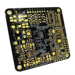
What Is a Low-Loss PCB?
A Low-Loss PCB is a printed circuit board designed and manufactured to minimize signal attenuation, dielectric loss, conductor loss, and other sources of transmission loss. These boards are particularly important in high-speed and high-frequency electronic systems where maintaining signal quality over the entire transmission path is critical.
As data rates and operating frequencies continue to increase, conventional PCB materials may introduce excessive dielectric and conductor losses. These losses can cause signal attenuation, distortion, timing errors, increased insertion loss, and reduced transmission distance.
Low-loss PCB technology addresses these challenges through a combination of advanced laminate materials, controlled impedance, optimized stackup structures, appropriate copper selection, precise manufacturing processes, and careful high-speed layout practices.
Low-Loss PCB Materials are commonly used in telecommunications, data centers, medical equipment, aerospace and defense systems, automotive electronics, RF and microwave products, and other applications where signal integrity is critical.
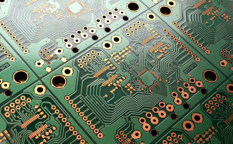
Why Do We Need Low-Loss PCBs?
Low-loss PCBs are generally more expensive than conventional PCB solutions, so why are they necessary?
The answer is closely related to signal frequency and data rate.
High-speed digital and high-frequency signals are more sensitive to transmission-line effects than low-frequency signals. As a signal travels through a PCB trace, part of its energy is lost because of dielectric loss, conductor loss, surface roughness, impedance discontinuities, and other factors.
If these losses become excessive, the receiver may have difficulty distinguishing between valid and invalid signal states. The result can include reduced eye opening, increased jitter, signal distortion, and higher bit-error rates.
This is especially important in modern applications such as 5G communication, high-speed Ethernet, PCIe, high-speed computing, radar, and RF systems.
The primary purpose of a Low-Loss PCB is therefore not simply to make the board “faster.” Instead, it is to maintain predictable electrical performance and Signal Integrity throughout the transmission path.
Key Factors Affecting Low-Loss PCB Performance
Several factors determine whether a PCB can achieve low transmission loss and reliable high-speed performance.
Material Selection
Material selection is one of the most important factors in designing a low-loss circuit board.
A suitable laminate should provide stable and predictable electrical properties across the operating frequency and temperature range.
Important characteristics include:
- Low and stable dielectric constant (Dk): Dielectric constant affects signal propagation velocity, impedance, and electrical delay. A stable Dk helps engineers maintain predictable transmission-line characteristics across the PCB.
- Low dissipation factor (Df): Also called loss tangent, Df represents the amount of energy dissipated within the dielectric material. A lower Df generally means lower dielectric loss, which is particularly important at high frequencies.
- Controlled coefficient of thermal expansion (CTE): A suitable CTE helps maintain dimensional stability and mechanical reliability during temperature changes and PCB processing.
- Good thermal conductivity: Improved thermal performance can help dissipate heat generated by high-power components and maintain stable operating conditions.
Common high-performance laminate families used in low-loss and high-frequency applications include advanced materials from Rogers, Isola, Panasonic, and other specialized material suppliers.
The appropriate material should be selected according to frequency, loss requirements, thermal conditions, impedance targets, board construction, and overall project cost.
Impedance Control
Impedance Control is essential for maintaining signal integrity in high-speed and high-frequency PCB designs.
PCB impedance is determined by multiple factors, including trace width, copper thickness, dielectric thickness, dielectric constant, conductor geometry, and the surrounding reference planes.
Two common types of controlled impedance are:
Single-Ended Impedance
Single-ended impedance refers to the impedance of an individual transmission line relative to its reference plane. It is commonly used in RF circuits, antenna structures, clocks, and various high-speed digital interfaces.
Differential Impedance
Differential impedance refers to the impedance between two coupled traces carrying complementary signals. Differential routing is widely used in interfaces such as USB, Ethernet, PCIe, HDMI, and other high-speed communication systems.
The required impedance depends on the interface specification. For example, many Ethernet systems use approximately 100 Ω differential impedance, while USB and other interfaces may use different target values.
Maintaining the specified impedance throughout the complete signal path helps reduce reflections, distortion, and transmission loss.
Poor impedance control can result in increased reflections, degraded eye diagrams, timing problems, and higher bit-error rates.
Copper and Conductor Characteristics
Copper is another important factor affecting PCB transmission loss.
At high frequencies, current tends to concentrate near the surface of a conductor because of the skin effect. As frequency increases, the effective area through which current flows becomes smaller, making conductor surface characteristics increasingly important.
Copper surface roughness can therefore influence high-frequency insertion loss. Using appropriate copper foil and controlling the copper surface during PCB manufacturing can help reduce unnecessary conductor loss.
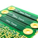
Copper thickness must also be selected according to current-carrying requirements, thermal conditions, mechanical requirements, and high-frequency performance.
PCB Layout and Routing
Even with an excellent low-loss laminate and precise impedance control, poor PCB layout can still degrade signal integrity.
Important routing practices include:
- Minimize unnecessary trace length.
- Avoid unnecessary vias and via stubs.
- Maintain consistent trace width.
- Use appropriate reference planes.
- Keep high-speed traces away from noisy circuits.
- Avoid abrupt changes in trace geometry.
- Minimize unnecessary branches and stubs.
- Match the length of differential pairs where required.
- Avoid unnecessary right-angle routing.
- Maintain appropriate spacing between sensitive signal paths.
For complex high-speed designs, engineers should evaluate the complete transmission path rather than focusing on the PCB trace alone.
Benefits of Low-Loss PCBs
A properly designed low-loss PCB can provide several important advantages.
Improved Signal Integrity
The primary benefit is improved Signal Integrity.
Low-loss materials and controlled transmission-line structures reduce signal attenuation and distortion, helping preserve signal quality over longer electrical paths.
This is particularly important when data rates and frequencies increase.
Better High-Speed and High-Frequency Performance
A High-Speed PCB must manage transmission-line effects such as reflection, crosstalk, insertion loss, and impedance discontinuity.
Low-loss materials can reduce dielectric loss and help maintain predictable electrical characteristics, making them suitable for demanding high-speed interfaces.
Similarly, a High-Frequency PCB requires materials with carefully controlled dielectric properties to maintain stable RF and microwave performance.
Reduced Transmission Loss
Lower dielectric loss and optimized conductor structures can reduce the amount of energy lost as a signal travels through the PCB.
This can be especially valuable in long transmission paths, high-frequency RF systems, and high-speed networking equipment.
Improved Thermal Management
Some high-performance PCB materials provide improved thermal characteristics. Combined with suitable copper structures, thermal vias, heat spreaders, and other thermal-management techniques, they can help control operating temperatures.
Lower operating temperatures can also contribute to improved long-term component and system reliability.
Increased System Reliability
Stable dielectric properties, controlled impedance, appropriate material selection, and precise manufacturing can reduce electrical variation between PCB lots.
This consistency is important for products requiring repeatable performance across large production volumes.
Support for High-Density Designs
Modern electronic systems often require more functions in a smaller physical area. High-density PCB designs can create additional challenges involving signal coupling, thermal management, and impedance control.
Low-loss materials combined with carefully engineered stackups can help designers meet these requirements without unnecessarily increasing board dimensions.
Applications of Low-Loss PCBs
Low-loss PCB technology is used in many industries where signal quality and transmission performance are critical.
Telecommunications
Telecommunication systems continue to move toward higher data rates and higher operating frequencies.
Applications such as 5G infrastructure, communication modules, routers, switches, and high-speed optical networking equipment can benefit from low-loss PCB materials and controlled impedance structures.
Data Centers
Modern data centers depend on high-speed servers, network switches, storage systems, and interconnects.
At high data rates, excessive insertion loss, crosstalk, jitter, and signal distortion can affect system performance.
Low-loss materials can therefore be used in high-speed networking and computing platforms to support reliable data transmission.
Medical Equipment
Medical imaging and diagnostic systems require accurate and stable signal transmission.
Equipment such as MRI systems, CT scanners, ultrasound systems, and other advanced medical electronics may contain high-speed, high-frequency, or sensitive analog circuits where signal integrity is critical.
Aerospace and Radar
Aerospace and defense electronics often operate under demanding electrical and environmental conditions.
Radar, satellite communication, navigation systems, avionics, and RF equipment can require low-loss materials and highly controlled impedance to maintain signal accuracy at high frequencies.
Automotive Electronics
Automotive electronics increasingly incorporate high-speed communication, radar, sensing, and advanced computing systems.
Low-loss PCB technology can be applied to automotive radar, ADAS systems, vehicle networking, infotainment, and other applications where high-frequency or high-speed signals must remain stable.
Consumer Electronics
Smartphones, wearables, laptops, networking products, and other compact electronic devices increasingly process high-speed data.
Low-loss PCB materials can help engineers manage signal integrity while maintaining compact board dimensions and efficient thermal performance.
Cost Factors of Low-Loss PCBs
Although low-loss PCBs generally cost more than standard circuit boards, the final cost depends on several design and manufacturing factors.
Selecting the Right Material
The cost of Low-Loss PCB Materials varies significantly according to their electrical performance.
PCB laminates can generally be categorized into standard-loss, low-loss, ultra-low-loss, and extremely-low-loss material classes.
Choosing a material with substantially better electrical performance than the application actually requires can increase cost without providing meaningful system-level benefits.
Engineers should therefore select the lowest-cost material that can reliably meet the application’s electrical requirements.
Surface Finish Selection
Surface finish can affect both cost and high-frequency performance.
The appropriate finish should be selected according to electrical requirements, solderability, reliability, environmental conditions, and assembly requirements.
Impedance Control Requirements
Tighter impedance tolerances require greater manufacturing precision and more extensive testing.
Trace width, dielectric thickness, copper thickness, and layer registration must all be tightly controlled.
Therefore, highly demanding impedance specifications can increase manufacturing costs.
Copper Requirements
Heavy copper may be necessary for high-current applications, but excessive copper can affect etching, impedance, thermal performance, and manufacturing complexity.
Copper thickness should therefore be optimized according to actual electrical and thermal requirements.
Testing and Quality Control
Advanced low-loss PCBs may require additional electrical testing, impedance testing, cross-section analysis, dimensional inspection, and material traceability.
These quality-control requirements should be considered when estimating total production costs.
Avoiding Unnecessary Over-Engineering
Not every high-speed design requires the most expensive laminate or the most advanced manufacturing technology.
The best approach is to balance electrical performance, reliability, manufacturability, and cost.
A well-engineered PCB uses advanced materials and technologies only where they provide measurable value.
Key Manufacturing Considerations for Low-Loss PCBs
The performance of a low-loss circuit board depends not only on the material but also on the quality and consistency of the manufacturing process.
Controlled Lamination
Multilayer low-loss PCBs require precise control of dielectric thickness and layer alignment.
Lamination parameters such as temperature, pressure, heating rate, and cooling conditions should be controlled according to the selected material system.
Precision Drilling
High-speed designs can be sensitive to via geometry and parasitic effects.
Drilling accuracy, hole quality, aspect ratio, and via structure should therefore be carefully controlled.
Accurate Etching
Trace width directly influences impedance. Variations introduced during etching can therefore affect high-speed electrical performance.
Precise etching and process monitoring are important for maintaining consistent trace geometry.
Controlled Copper Plating
Copper thickness affects resistance, impedance, thermal performance, and mechanical reliability.
Consistent plating is particularly important when tight impedance tolerances are required.
Electrical Testing
Depending on the product requirements, PCB Manufacturing may include automated electrical testing, controlled impedance testing, flying-probe testing, and other inspection methods.
For demanding high-frequency products, network-analyzer-based measurements may also be used during qualification and engineering validation.
How Kingda Supports Low-Loss PCB Manufacturing
For a low-loss PCB project, selecting the right laminate is only the first step. Material properties must be coordinated with PCB stackup, trace geometry, impedance requirements, manufacturing processes, and testing methods.
Kingda can support customers in developing low-loss PCB solutions according to application frequency, data rate, layer count, dielectric thickness, impedance requirements, thermal conditions, and mechanical constraints.
The engineering process can include material evaluation, stackup optimization, controlled impedance design, manufacturing review, and quality inspection.
For demanding high-speed and high-frequency applications, Kingda focuses on maintaining consistency throughout the PCB Manufacturing process so that the selected material and PCB structure can deliver predictable electrical performance.
How to Choose the Right Low-Loss PCB
Before ordering a low-loss PCB, engineers should clearly define the electrical and mechanical requirements of the project.
Consider the following factors:
- Operating frequency: Determine the actual frequency range and data rate.
- Signal-loss requirements: Define acceptable insertion loss and attenuation.
- Material properties: Evaluate Dk, Df, CTE, thermal characteristics, and thickness.
- Impedance requirements: Define single-ended and differential impedance targets.
- PCB stackup: Optimize signal layers and reference planes.
- Copper configuration: Select suitable copper thickness and surface characteristics.
- Manufacturing capability: Confirm that the manufacturer can achieve the required tolerances.
- Testing requirements: Determine whether impedance, electrical, thermal, or other specialized testing is required.
- Cost target: Select a material and process that provide sufficient performance without unnecessary over-engineering.
Conclusion
A Low-Loss PCB is an important solution for modern electronic systems that require reliable transmission of high-speed or high-frequency signals. Compared with conventional PCB materials, low-loss technologies can provide lower dielectric loss, improved signal integrity, more predictable impedance, and better performance in demanding applications.
The overall performance of a low-loss circuit board depends on more than the laminate itself. Material selection, Impedance Control, copper characteristics, PCB stackup, routing, manufacturing precision, and testing must all work together.
As technologies such as 5G, high-speed Ethernet, advanced computing, automotive radar, aerospace electronics, and medical systems continue to evolve, the demand for Low-Loss PCB Materials will continue to grow.
By selecting the appropriate material and partnering with an experienced manufacturer such as Kingda, engineers can achieve the right balance between signal performance, reliability, manufacturability, and cost.