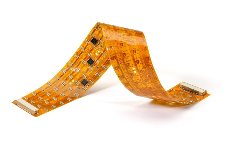
As electronic devices become smaller, lighter, and more functionally integrated, flexible circuits are increasingly used in applications where conventional rigid circuit boards cannot provide sufficient mechanical flexibility or space efficiency. Flexible PCB Assembly combines flexible circuit technology with electronic component assembly to create compact, lightweight, and reliable electronic modules.
Unlike conventional rigid PCBs, a Flexible PCB is designed to bend, fold, or flex within specified mechanical limits. This makes flexible circuits particularly useful for compact electronic products, automotive systems, medical devices, aerospace equipment, wearable electronics, and other applications where space is limited or the circuit must conform to a specific shape.
Kingda provides PCB manufacturing and assembly support for flexible circuit applications, with production processes designed around the mechanical, electrical, and assembly requirements of each project. From prototype development to volume production, proper material selection, fixture design, process control, inspection, and testing are essential for achieving reliable Flexible PCB Assembly results.
What Is Flexible PCB Assembly?
Flexible PCB Assembly is the process of mounting and soldering electronic components onto a flexible printed circuit board.
A typical Flex PCB uses a flexible dielectric substrate, most commonly polyimide, together with copper conductors. The copper is patterned through PCB fabrication processes to form the required circuit. A coverlay or other protective layer is then applied to protect the conductors and provide electrical insulation.
Depending on the application, a flexible circuit may be manufactured as a single-layer, double-layer, or multilayer structure. It may also incorporate features such as stiffeners, plated through-holes, blind vias, or other specialized structures.
The flexible substrate provides mechanical flexibility, while stiffeners may be added in specific areas to improve dimensional stability or provide adequate support for connectors and component mounting.
During assembly, the flexible PCB must be handled differently from a rigid PCB because the thin substrate can move, bend, or deform during manufacturing. Specialized fixtures or carriers are therefore commonly used to maintain the board’s flatness and position during solder paste printing, component placement, inspection, and other processes.
Advantages of Flexible PCB Assembly
Flexible circuits provide several advantages over conventional rigid PCBs, especially when products require compact packaging or three-dimensional circuit routing.
Flexibility
The primary advantage of a flexible circuit is its ability to bend and conform to different mechanical shapes.
A flexible circuit can be routed around corners, folded into compact spaces, or positioned along curved surfaces. This can simplify product architecture and reduce the need for multiple rigid boards and wire harnesses.
However, flexibility must always be considered within the mechanical design limits of the material. Repeated bending, bend radius, copper type, layer structure, and bend location can all affect long-term reliability.
Lightweight and Thin Construction
A Flexible PCB is generally thinner and lighter than an equivalent rigid PCB assembly.
This makes flexible circuits attractive for portable electronics, wearable devices, compact sensors, displays, cameras, and other applications where weight and package thickness are important design considerations.
Space Efficiency
Because a flexible circuit can be folded or shaped during final assembly, it can occupy less three-dimensional space than a rigid board.
This is particularly valuable in products with limited internal space, where the circuit must pass through narrow or irregular areas.
Improved Mechanical Integration
Flexible circuits can integrate electrical connections into mechanical structures more efficiently.
For example, a flexible circuit can connect two modules located at different angles without requiring a separate cable assembly or connector in certain applications.
Reducing connectors and cable assemblies may also simplify system integration and reduce the number of individual components.
Resistance to Certain Environmental Conditions
Polyimide is widely used in flexible circuits because of its useful thermal and chemical characteristics.
Depending on the selected material system and construction, flexible circuits can be designed for demanding environments involving temperature variation, vibration, and mechanical movement. The actual environmental capability, however, depends on the complete material stackup and assembly design rather than the substrate alone.
Applications of Flexible PCB Assembly
Flexible PCB Assembly is used across a wide range of industries.
Consumer Electronics
Flexible circuits are widely used in smartphones, tablets, cameras, displays, wearable devices, laptops, and other compact electronic products.
They can provide electrical connections between closely packed modules while allowing the circuit to follow the internal geometry of the product.
Automotive Electronics
Automotive electronics increasingly require compact and lightweight electrical connections.
Flexible circuits can be used in sensors, cameras, display systems, lighting modules, instrument clusters, infotainment systems, battery-related electronics, and other vehicle subsystems.
Their ability to accommodate vibration and complex mechanical packaging makes them useful for applications where conventional rigid boards or cable assemblies may be difficult to integrate.
Medical Electronics
Medical devices often require compact electronics with reliable electrical connections.
Flexible circuits can be found in applications such as wearable medical equipment, diagnostic devices, monitoring equipment, hearing-related electronics, and other space-constrained systems.
For medical products, material selection, cleanliness, reliability, and applicable regulatory requirements must be evaluated according to the end application.
Aerospace and Defense
Aerospace electronics can place demanding requirements on weight, space, vibration resistance, and environmental performance.
Flexible circuits can reduce wiring volume and support complex packaging in avionics, sensors, instrumentation, and other aerospace systems.
The appropriate material system and qualification requirements should be selected according to the operating environment.
Flexible PCB Assembly Process
The basic PCB Assembly process for flexible circuits is similar to SMT assembly for rigid boards. However, the flexible substrate introduces additional process-control requirements.
A typical process includes:
- Material and PCB preparation
- Fixture or carrier preparation
- Solder paste printing
- Solder paste inspection
- Component placement
- Reflow soldering
- AOI inspection
- Through-hole or secondary assembly when required
- Electrical testing
- Final inspection and packaging
Each stage must account for the mechanical characteristics of the flexible substrate.
Solder Paste Printing
Solder paste printing is one of the most critical stages in SMT Assembly.
Unlike a rigid PCB, a flexible circuit may not remain perfectly flat during printing. Even small amounts of movement or deformation can affect stencil contact and solder paste deposition.
A carrier or dedicated fixture is therefore commonly used to support the flexible circuit and maintain a stable surface.
The stencil design, aperture dimensions, solder paste type, printing pressure, squeegee speed, and separation parameters should be optimized according to the PCB design and component requirements.
Polyimide materials can also absorb moisture, so appropriate material storage and preconditioning procedures should be established according to the material manufacturer’s recommendations. Baking should not be treated as a universal fixed-temperature process; the required temperature and duration depend on the material construction and applicable specifications.
Component Placement
After solder paste printing, automated pick-and-place equipment positions the components on the flexible circuit.
Machine vision systems are used to identify component locations and verify placement accuracy.
Because flexible circuits can move during processing, the carrier and positioning system must provide sufficient support and repeatability.
Component placement considerations include:
- Component package type
- Component weight
- Placement accuracy
- Pad design
- Board-to-carrier alignment
- Component orientation
- Mechanical stress around solder joints
Components located in areas that will experience repeated bending should receive particular attention during mechanical and electrical design.
Reflow Soldering
During reflow soldering, the assembled flexible PCB passes through a controlled thermal profile.
The solder paste is heated until it reaches the appropriate melting temperature, allowing the solder to wet the component leads and PCB pads. The board is then cooled under controlled conditions to form the final solder joints.
The reflow profile should be established based on the solder paste manufacturer’s recommendations, component temperature limitations, PCB materials, and assembly requirements.
For flexible circuits, excessive thermal stress or uneven heating may contribute to substrate deformation or assembly defects. Process validation is therefore important, particularly for thin or complex flexible structures.
Thermocouple measurements can be used during process development to verify the actual temperature experienced by critical components and PCB areas.
AOI Inspection
AOI Inspection is commonly used after reflow soldering to detect visible assembly defects.
Depending on the equipment and programming, AOI can identify issues such as:
- Missing components
- Incorrect component placement
- Component polarity errors
- Solder bridges
- Insufficient or excessive solder
- Misalignment
- Visible soldering defects
Flexible PCB inspection can be more challenging than rigid-board inspection because the substrate may have different reflective characteristics and can be more difficult to keep perfectly flat.
Using an appropriate fixture or carrier helps improve inspection consistency.
AOI cannot reliably inspect every type of hidden solder joint. For components such as BGA packages, X-ray inspection may be required when hidden solder-joint verification is necessary.
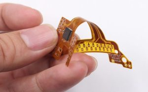
PCB Testing
Visual inspection and AOI cannot identify every electrical problem. PCB Testing is therefore an important part of the assembly process.
Common testing methods include:
In-Circuit Test
ICT uses a fixture with multiple test points to check electrical characteristics and circuit connections.
It can provide efficient testing for production volumes that justify dedicated test fixtures.
Flying-Probe Testing
Flying-probe testing uses movable probes to contact designated test points on the PCB.
It generally provides greater flexibility than ICT for prototypes and lower-volume production because a dedicated bed-of-nails fixture may not be required.
Functional Testing
Functional testing evaluates whether the completed assembly performs according to its intended electrical and system requirements.
The exact test procedure depends on the product and may include power-up testing, communication checks, sensor verification, signal measurement, or system-level operation.
Special Considerations for Flexible PCB Assembly
Flexible circuits require additional attention during design and manufacturing.
Bend Radius
The minimum bend radius is an important mechanical parameter.
Repeated bending should be evaluated differently from one-time folding during installation. Excessive bending can damage copper conductors, plated structures, solder joints, or the dielectric material.
The allowable bend radius depends on factors such as:
- Copper thickness
- Number of conductive layers
- Material construction
- Static or dynamic bending
- Bend direction
- Coverlay structure
- Stiffener placement
Stiffener Design
Stiffeners can be added to selected areas of a flexible circuit to improve mechanical strength.
They are commonly used around connectors, component-mounting regions, and other locations where additional support is required.
However, stiffeners should be positioned carefully because they change the mechanical behavior of the flexible circuit.
Component Placement
Large or heavy components should generally not be placed in areas expected to undergo repeated flexing.
Critical components and solder joints should be positioned in mechanically stable areas whenever possible.
Copper Routing
Copper traces in flexing regions should be designed with mechanical reliability in mind.
Sharp corners, unnecessary stress concentrations, and unsuitable conductor geometries can increase the risk of fatigue during repeated bending.
The PCB designer should define the flexing area clearly and coordinate the electrical layout with the mechanical design.
Common Flexible PCB Assembly Defects
Several defects may occur if flexible circuits are not properly supported or the assembly process is not adequately controlled.
| Defect | Possible Cause | Preventive Measure |
|---|---|---|
| Solder bridging | Excessive solder paste or poor printing | Optimize stencil and printing parameters |
| Insufficient solder | Insufficient paste deposition | Improve stencil and SPI control |
| Component misalignment | Board movement or placement error | Improve fixture and placement accuracy |
| Tombstoning | Uneven solder wetting | Optimize pad design and reflow profile |
| Warpage or deformation | Inadequate support or thermal stress | Use appropriate carriers and thermal control |
| Cracked solder joints | Excessive mechanical stress | Review component placement and flexing areas |
| Electrical open | Damaged trace or poor solder joint | Perform appropriate electrical testing |
How to Improve Flexible PCB Assembly Quality
A reliable PCB Manufacturing and assembly process begins before the board enters production.
Several practices can improve manufacturing consistency:
- Perform DFM and assembly design reviews before production.
- Clearly define static and dynamic flexing areas.
- Select materials according to electrical and mechanical requirements.
- Use appropriate stiffeners where additional support is required.
- Design suitable fixtures for printing, placement, and inspection.
- Control solder paste storage and printing conditions.
- Validate the reflow temperature profile.
- Use AOI and other appropriate inspection methods.
- Apply electrical testing according to product requirements.
- Verify packaging and handling procedures to prevent mechanical damage.
Flexible PCB Assembly vs. Rigid PCB Assembly
| Feature | Flexible PCB Assembly | Rigid PCB Assembly |
|---|---|---|
| Substrate | Flexible materials such as polyimide | Rigid materials such as FR-4 |
| Mechanical flexibility | High | Very limited |
| Weight | Generally lower | Generally higher |
| Packaging | Suitable for compact and three-dimensional structures | Best suited to fixed planar structures |
| Fixture requirements | Often requires specialized support | Usually simpler |
| Design considerations | Bend radius, flex area, stiffeners | Board rigidity and mechanical mounting |
| Typical applications | Wearables, cameras, automotive, medical, aerospace | Computers, industrial equipment, power electronics |
Neither technology is universally better. The appropriate choice depends on the product’s electrical, mechanical, thermal, manufacturing, and cost requirements.
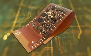
Kingda Flexible PCB Assembly Services
Kingda supports flexible circuit manufacturing and assembly projects according to customer-specific design and production requirements.
For each project, important factors such as flexible substrate construction, copper thickness, layer count, component density, stiffener requirements, bending conditions, assembly method, inspection requirements, and testing specifications should be reviewed before production.
Kingda can support assembly processes such as SMT Assembly, through-hole assembly where applicable, reflow soldering, AOI Inspection, and electrical PCB Testing according to project requirements.
For prototype and production projects, engineering review and manufacturing coordination are particularly important. A properly prepared manufacturing package, accurate BOM, suitable component footprints, and clear assembly drawings can reduce production risks and improve overall efficiency.
Conclusion
Flexible PCB Assembly enables electronic designers to integrate reliable electrical connections into products where conventional rigid circuit boards may be difficult to use.
The major advantages of flexible circuits include flexibility, low weight, thin construction, space efficiency, and improved mechanical integration. These characteristics make them suitable for consumer electronics, automotive systems, medical equipment, aerospace products, wearable devices, and many other compact electronic applications.
At the same time, flexible circuits require specialized attention during PCB Assembly. Fixture design, solder paste printing, component placement, reflow control, AOI Inspection, mechanical design, and PCB Testing all influence final product quality.
By considering the flexible circuit’s mechanical behavior from the design stage and coordinating PCB fabrication with assembly requirements, manufacturers can achieve a more stable and reliable production process. For projects requiring compact packaging, mechanical flexibility, and dependable electrical performance, flexible PCB technology provides an effective alternative to conventional rigid circuit boards.