I-Tera MT40 PCB: PCB Design, PCB Manufacturing, High-Speed & RF Applications
As electronic systems continue to demand higher data rates, greater efficiency, lower signal loss, and improved reliability, advanced PCB materials have become increasingly important. Conventional FR-4 materials remain suitable for a wide range of applications, but demanding high-speed digital, RF, microwave, and high-frequency designs often require tighter control of dielectric properties and transmission losses.
I-Tera® MT40 from Isola is a very-low-loss laminate and prepreg system developed for high-speed digital and RF/microwave PCB applications. It combines a stable dielectric constant (Dk), low dissipation factor (Df), high thermal reliability, CAF resistance, and compatibility with conventional FR-4-style PCB manufacturing processes.
According to Isola, standard I-Tera MT40 has a typical Dk of 3.45, Df of 0.0031, Tg of 215°C, Td of 360°C, and thermal conductivity of 0.61 W/m·K. The material is designed to provide a practical alternative to PTFE and other specialized high-frequency materials while maintaining compatibility with conventional PCB processing.
This article examines I-Tera MT40’s electrical and thermal properties, manufacturing advantages, PCB Design considerations, and applications in high-speed computing, telecommunications, automotive electronics, medical systems, aerospace, and other advanced electronic products.
What Is I-Tera MT40?
I-Tera MT40 is a high-speed, very-low-loss laminate and prepreg material designed for demanding digital and RF/microwave printed circuit applications.
Unlike conventional PCB materials that may introduce greater dielectric loss at higher frequencies, MT40 provides a relatively low Df and stable dielectric behavior across a broad frequency and temperature range. This makes it useful for applications where signal integrity, impedance control, and transmission efficiency are critical.
Isola describes I-Tera MT40 as suitable for high-speed digital and RF/microwave PCB designs. Its stable Dk and low Df allow designers to develop controlled-impedance transmission structures without necessarily moving to PTFE-based manufacturing processes.
Another important advantage is process compatibility. MT40 can be processed using many conventional PCB manufacturing methods, including lamination, drilling, plating, soldering, and multilayer fabrication. Isola specifically identifies the material as FR-4 process compatible, multiple-reflow capable, and suitable for multiple lamination cycles.
Key I-Tera MT40 Material Properties
The following table summarizes representative properties of standard I-Tera MT40 based on Isola’s published technical information.
| Property | Typical Value |
|---|---|
| Dielectric Constant (Dk) | 3.45 |
| Dissipation Factor (Df) | 0.0031 |
| Glass Transition Temperature (Tg) | 215°C |
| Decomposition Temperature (Td) | 360°C |
| Thermal Conductivity | 0.61 W/m·K |
| X/Y-Axis CTE, Pre-Tg | 12 ppm/°C |
| Z-Axis CTE, Pre-Tg | 55 ppm/°C |
| Z-Axis CTE, Post-Tg | 290 ppm/°C |
| Dielectric Breakdown | 45.4 kV |
| Volume Resistivity | 1.33 × 10⁷ MΩ·cm |
| Surface Resistivity | 1.33 × 10⁵ MΩ |
| Moisture Absorption | 0.1% |
| Flammability | UL 94 V-0 |
| Thermal Conductivity Test | ASTM E1952 |
These are typical material values rather than guaranteed production values. Actual PCB performance depends on resin content, glass style, copper roughness, construction, fabrication tolerances, frequency, temperature, and the specific MT40 construction selected.
For RF/microwave configurations, Isola also lists MT40 variants with Dk values of approximately 3.38, 3.45, 3.60, and 3.75 and Df values ranging from 0.0028 to 0.0035 at 10 GHz, depending on the selected construction.
Major Characteristics of I-Tera MT40
Stable Dielectric Constant
One of the most important advantages of MT40 is its stable dielectric behavior.
For controlled-impedance PCB Design, Dk directly affects transmission-line impedance and propagation characteristics. A predictable dielectric constant helps engineers establish more reliable stackups and impedance targets.
Isola states that I-Tera MT40 maintains stable dielectric properties across a broad temperature and frequency range. The standard MT40 material is specified for stability from -55°C to +125°C up to W-band frequencies, while the RF/MW version has a different published temperature range depending on construction.
This stability is particularly valuable for:
- High-speed differential pairs
- RF transmission lines
- Microwave circuits
- Antenna feed networks
- High-speed SerDes channels
- Controlled-impedance multilayer PCBs
Very Low Dissipation Factor
The dissipation factor of standard MT40 is approximately 0.0031.
A lower Df generally means lower dielectric loss, particularly when transmission lines operate at higher frequencies. Reducing dielectric loss can help preserve signal amplitude and waveform quality across long electrical paths.
This characteristic makes MT40 attractive for demanding applications such as high-speed networking, telecommunications, RF equipment, radar-related electronics, and high-performance computing.
However, material Df is only one part of the total channel-loss budget. Copper roughness, conductor geometry, trace length, connector transitions, vias, glass weave effects, and other discontinuities can also influence high-speed signal performance.
High Thermal Reliability
MT40 has a typical Tg of 215°C and Td of 360°C in Isola’s current standard material data. The material also demonstrates strong thermal resistance during PCB processing.
This thermal performance is important for lead-free assembly and multilayer fabrication because modern PCBs may experience repeated thermal cycles during:
- Lamination
- Reflow soldering
- Rework
- Component assembly
- Multiple PCB processing stages
A high Tg does not mean the PCB can continuously operate at that temperature. Instead, Tg indicates a major transition in the polymer system, while actual operating temperature must be determined from the complete design, reliability requirements, and applicable specifications.
CAF Resistance and Long-Term Reliability
Conductive anodic filament (CAF) is an important reliability concern in densely routed multilayer PCBs, particularly when moisture, electrical bias, and closely spaced conductive structures are present.
MT40 is identified by Isola as CAF resistant and suitable for demanding multilayer applications.
For high-density PCB Manufacturing, CAF resistance can be particularly important when a design includes:
- Closely spaced vias
- Fine-pitch BGA packages
- High layer counts
- Small dielectric spacing
- High operating humidity
- Long service life requirements
Material selection should still be combined with appropriate PCB fabrication controls, via quality, cleanliness, moisture management, and spacing requirements.
FR-4 Process Compatibility
One of MT40’s strongest manufacturing advantages is that it does not require the same specialized processing approach associated with many PTFE-based materials.
Isola identifies MT40 as FR-4 process compatible, multiple-reflow capable, and capable of supporting multiple lamination cycles.
This can reduce the manufacturing barrier for PCB manufacturers that already have conventional multilayer production capabilities.
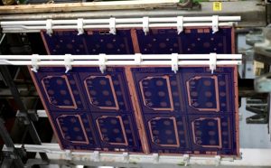
The practical benefits may include:
- Conventional lamination equipment
- Standard multilayer PCB processing
- Conventional drilling and plating
- Standard solder mask processing
- Standard SMT assembly workflows
- Easier integration into existing manufacturing systems
I-Tera MT40 vs. Conventional FR-4
Traditional FR-4 remains one of the most widely used PCB materials because of its balanced cost, mechanical properties, electrical performance, and manufacturing availability.
However, as signal frequencies and data rates increase, dielectric loss and impedance stability become more important.
| Characteristic | Conventional FR-4 | I-Tera MT40 |
|---|---|---|
| Typical Use | General-purpose electronics | High-speed and RF/microwave electronics |
| Dk | Material-dependent | 3.45 typical |
| Df | Material-dependent and generally higher than MT40 | 0.0031 typical |
| Signal Loss | Application-dependent | Lower-loss architecture |
| Thermal Reliability | Material-dependent | Tg 215°C typical |
| High-Speed Applications | Moderate to high depending on grade | Specifically designed for high-speed applications |
| RF/Microwave Applications | Limited by material grade | Suitable |
| Manufacturing | Conventional PCB processes | FR-4 process compatible |
| Cost | Generally lower | Higher than standard FR-4 |
| Design Control | Depends strongly on material grade | Improved dielectric predictability |
The choice should not be based simply on whether a material has a lower Dk or Df. Engineers should evaluate the complete channel-loss budget, impedance requirements, operating temperature, stackup, copper roughness, fabrication tolerances, and total system cost.
I-Tera MT40 in PCB Design

Using MT40 successfully requires more than simply replacing an FR-4 material in an existing design.
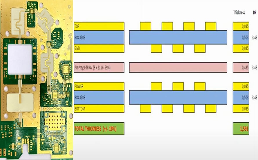
Optimize the PCB Stackup
A controlled multilayer stackup is fundamental to high-speed and RF PCB performance.
The stackup should define:
- Signal-layer locations
- Ground-plane locations
- Power-plane locations
- Dielectric thickness
- Copper thickness
- Glass styles
- Resin content
- Controlled impedance
- Via structures
- Differential-pair geometry
For high-speed signals, placing a solid reference plane close to the signal layer can provide a predictable return path and help control electromagnetic coupling.
Control Trace Impedance
MT40’s predictable dielectric properties can support controlled-impedance designs.
Typical controlled structures include:
- Microstrip
- Stripline
- Coplanar waveguide
- Differential transmission lines
- RF transmission lines
However, designers should not calculate impedance using Dk alone. Actual impedance depends on dielectric thickness, conductor width, copper thickness, copper roughness, geometry, and the specific material construction.
For demanding designs, the final stackup should be modeled using fabrication-specific material data and, where necessary, a field solver.
Optimize Via Structures
Vias can introduce discontinuities into high-speed channels.
As data rates increase, via capacitance, inductance, antipads, via stubs, and reference-plane transitions can affect insertion loss and return loss.
Depending on the design, engineers may consider:
- Smaller via stubs
- Backdrilling
- Blind vias
- Buried vias
- Microvias
- Optimized antipad geometry
- Improved reference-plane transitions
These technologies can improve electrical performance but may also increase PCB Manufacturing complexity and cost.
Consider Glass-Weave Effects
Even with a low-loss laminate, high-speed differential pairs can experience skew or local dielectric variation associated with the glass/resin structure.
For particularly sensitive channels, designers should evaluate:
- Trace orientation
- Glass style
- Resin distribution
- Differential-pair symmetry
- Routing density
- Channel length
The appropriate strategy depends on the actual stackup and frequency range.
Thermal Management with MT40
Although MT40 offers a thermal conductivity of approximately 0.61 W/m·K, it should not be treated as a high-thermal-conductivity PCB substrate in the same category as dedicated metal-core or thermally enhanced ceramic materials.
Thermal performance still depends heavily on the complete PCB architecture.
Effective thermal strategies may include:
- Large copper planes
- Thermal vias
- Copper pours
- Heat spreaders
- Thermal interface materials
- Component placement optimization
- External heatsinks
- Adequate airflow
- Short thermal paths
For high-power RF or digital systems, electrical and thermal design should be considered together.
I-Tera MT40 PCB Manufacturing Process
MT40 can be incorporated into a conventional multilayer PCB Manufacturing workflow.
A typical process may include:
- Material selection and stackup definition
- Inner-layer imaging
- Inner-layer etching
- AOI inspection
- Layup and lamination
- Mechanical or laser drilling where appropriate
- Desmear and hole preparation
- Electroless copper deposition
- Copper electroplating
- Outer-layer imaging and etching
- Solder mask application
- Surface finishing
- Silkscreen printing
- Routing or profiling
- Electrical testing
- Final inspection and reliability verification
The exact process depends on the layer count, via technology, copper thickness, surface finish, impedance requirements, and HDI construction.
Because MT40 is designed to be FR-4 process compatible, manufacturers can integrate it into established production infrastructure rather than adopting an entirely separate PTFE manufacturing process.
Manufacturing and Compliance Advantages
MT40 provides several advantages beyond its electrical performance.
Multiple Lamination and Reflow Capability
Modern high-density boards may require sequential lamination, multiple assembly operations, and lead-free reflow.
MT40 is identified as capable of multiple lamination cycles and multiple reflow processes, making it suitable for complex multilayer and HDI structures.
Dimensional Stability
Dimensional stability is important for fine-line routing, microvias, BGA registration, and multilayer alignment.
The material’s published X/Y-axis CTE is approximately 12 ppm/°C before Tg, supporting dimensional control when the complete manufacturing process is properly managed.
RoHS and UL Recognition
Isola lists MT40 as RoHS compliant and identifies UL File E41625. The standard material is also listed with UL 94 V-0 flammability performance and IPC-4103/17 and IPC-4101/102 recognition.
Compliance should always be confirmed against the specific material construction, revision, customer specification, and applicable end-product requirements.
Applications of I-Tera MT40
High-Speed Computing and Data Centers
Modern servers, switches, storage systems, and high-performance computing platforms rely on high-speed serial interfaces.
As channel frequencies and data rates increase, insertion loss, return loss, crosstalk, impedance discontinuities, and dielectric loss become increasingly important.
MT40 can therefore be considered for high-speed multilayer boards used in:
- Network switches
- Servers
- Data storage
- High-speed computing
- Communication backplanes
- High-speed interface boards
The material’s low Df and stable Dk can help engineers develop lower-loss transmission channels.
5G and Telecommunications
Telecommunications equipment frequently combines high-speed digital processing with RF and microwave circuits.
MT40 is particularly relevant to designs where low-loss transmission and stable dielectric properties are important, including RF front ends, communication equipment, wireless infrastructure, and other high-frequency systems.
The RF/MW version is specifically positioned by Isola for RF and microwave PCB applications.
Automotive Electronics
Modern vehicles increasingly rely on high-speed communication, radar-related electronics, ADAS, and electrified powertrain systems.
MT40 may be considered for automotive applications where electrical performance and thermal reliability are important.
Potential applications include:
- Automotive radar
- ADAS control electronics
- High-speed vehicle networking
- Infotainment systems
- Communication modules
- Electrified vehicle electronics
Automotive qualification should be evaluated at the complete product level rather than inferred from laminate properties alone.
Aerospace and Defense
Aerospace and defense electronics often require stable electrical performance over demanding environmental conditions.
Potential applications for low-loss high-speed laminates include:
- Radar electronics
- Avionics
- Satellite communication
- High-frequency instrumentation
- Defense communication systems
- Electronic sensing systems
In these applications, material selection must be combined with environmental qualification, mechanical reliability, thermal cycling, vibration, and applicable industry standards.
Medical Electronics
Medical imaging and diagnostic systems can require high-speed data acquisition and sensitive signal processing.
Potential applications include:
- MRI-related electronics
- CT systems
- X-ray equipment
- Ultrasound systems
- Wireless medical devices
- Diagnostic instrumentation
Isola’s medical and instrumentation materials portfolio includes MT40 among materials positioned for medical applications, including imaging and wireless systems.
How to Select MT40 for a PCB Project
Before selecting MT40, engineers should evaluate several factors.
1. Determine the Required Electrical Performance
Identify:
- Maximum operating frequency
- Data rate
- Channel length
- Insertion-loss budget
- Return-loss requirements
- Target impedance
- Differential-pair requirements
2. Define the Stackup
The stackup should specify:
- Number of layers
- Dielectric thickness
- Copper weight
- Glass style
- Resin content
- Signal-reference-plane relationships
3. Evaluate Manufacturing Capability
Confirm that the PCB manufacturer can support:
- Fine-line fabrication
- Controlled impedance
- HDI microvias
- Sequential lamination
- Backdrilling
- Advanced inspection
- Electrical testing
4. Consider Total Cost
MT40 can provide substantial electrical advantages, but material cost may be higher than standard FR-4.
Therefore, it should be used where the performance benefit justifies the additional material and fabrication cost.
5. Validate the Final PCB
Prototype testing should verify:
- Impedance
- Insertion loss
- Return loss
- Crosstalk
- Thermal performance
- Mechanical reliability
- Electrical isolation
- Environmental reliability
Why Choose a Professional PCB Manufacturing Partner?
Selecting the correct laminate is only one part of a successful high-speed PCB project.
A capable manufacturing partner should understand the relationship between material properties, stackup design, fabrication tolerances, impedance control, drilling, plating, solder mask, surface finish, and final electrical testing.
Kingda can support customers with PCB manufacturing and assembly requirements where material selection, high-speed performance, manufacturing reliability, and production consistency need to be considered together.
For MT40 projects, a manufacturing review should ideally begin before fabrication with:
- DFM analysis
- Stackup review
- Impedance planning
- Material verification
- Drill and via review
- Copper-thickness verification
- Manufacturing-tolerance evaluation
- Test-plan definition
This approach helps reduce redesigns and ensures that the selected laminate is properly translated into a manufacturable PCB structure.
Common Mistakes When Using I-Tera MT40
Treating MT40 as a Simple FR-4 Replacement
MT40 is FR-4 process compatible, but that does not mean every FR-4 stackup can simply be copied without modification.
The dielectric thickness, resin content, glass style, copper roughness, and impedance model must be reconsidered.
Focusing Only on Dk
A low or stable Dk is useful, but signal performance also depends on Df, conductor loss, copper roughness, geometry, vias, connectors, and return paths.
Ignoring Manufacturing Tolerances
A theoretically perfect impedance calculation may not match production results if dielectric thickness, trace width, copper thickness, and etching vary significantly.
Therefore, fabrication tolerances should be incorporated into the design from the beginning.
Assuming Low Loss Eliminates All Signal-Integrity Problems
MT40 can reduce dielectric loss, but it cannot automatically eliminate:
- Crosstalk
- Reflections
- Via discontinuities
- Poor return paths
- Connector losses
- Ground discontinuities
- EMI problems
Material selection and PCB Design must work together.
I-Tera MT40 vs. PTFE: Which Should You Choose?
MT40 is often positioned as a cost-effective alternative to PTFE and other commercial microwave and high-speed laminate materials.
However, the best material depends on the application.
MT40 can be attractive when a project requires:
- Low dielectric loss
- Stable dielectric properties
- High-speed digital performance
- RF/microwave capability
- Conventional PCB processing
- Multilayer construction
- Multiple reflow cycles
- Reasonable manufacturing complexity
PTFE-based materials may still be preferred for specialized microwave designs where extremely low loss or specific RF performance characteristics justify more specialized processing.
The correct selection should therefore be based on frequency, loss budget, impedance requirements, thermal environment, mechanical constraints, fabrication capability, and cost.
Conclusion
I-Tera MT40 is a high-performance PCB laminate and prepreg system designed for demanding high-speed digital and RF/microwave applications. Its combination of approximately 3.45 Dk, 0.0031 Df, 215°C Tg, 360°C Td, CAF resistance, and FR-4 process compatibility makes it an attractive option for advanced PCB applications.
For engineers working on high-speed networking, telecommunications, automotive electronics, aerospace systems, medical equipment, and other demanding electronic platforms, MT40 can provide a useful balance between electrical performance and manufacturability.
The most important point is that material selection should not be isolated from PCB Design and PCB Manufacturing. Stackup construction, impedance control, signal routing, via design, copper roughness, fabrication tolerances, thermal management, and final testing all contribute to actual PCB performance.
When these factors are considered together, MT40 can help manufacturers develop reliable, low-loss, high-speed circuit boards without requiring the highly specialized processing often associated with PTFE-based materials.
Article Summary
I-Tera MT40 is a very-low-loss laminate and prepreg material developed for high-speed digital and RF/microwave PCB applications. Its stable dielectric characteristics, low dissipation factor, high Tg, high Td, CAF resistance, and FR-4 process compatibility make it suitable for demanding multilayer PCB applications. For successful implementation, engineers should combine appropriate material selection with optimized stackup design, controlled impedance, high-speed routing, thermal management, DFM analysis, and comprehensive electrical testing.