Many engineers complete impedance simulation, determine trace widths, and finalize the stackup based on nominal material parameters. However, significant impedance variation may only become apparent after mass production begins. Impedance can vary from board to board and even across different regions of the same PCB.
Although trace etching and copper thickness variation can contribute to this problem, PCB Dielectric Tolerance is another major factor that should be evaluated during impedance design. Variations in dielectric thickness and dielectric constant can shift the electrical distance between a signal trace and its reference plane, resulting in measurable impedance changes.
Therefore, impedance design should not be based solely on nominal values. Engineers should systematically evaluate material tolerances, establish an impedance tolerance budget, and perform worst-case analysis before production. This approach helps improve impedance consistency and reduce the risk of large-scale PCB rework.
1. Two Major Types of PCB Dielectric Tolerance
The two most important dielectric variables in impedance-controlled PCB design are Dielectric Thickness and Dielectric Constant (Dk).
Dielectric Thickness Tolerance
Dielectric thickness is influenced by the construction and manufacturing process of the PCB.
For example, core materials have a specified thickness tolerance, while prepreg thickness after lamination depends on resin content, copper distribution, pressure, temperature, and lamination conditions.
The final dielectric thickness between a signal layer and its reference plane may therefore differ from the nominal value used in the original impedance calculation.
For a typical transmission-line structure, a change in dielectric thickness changes the electromagnetic relationship between the signal conductor and reference plane. As a result, the characteristic impedance also changes.
The actual tolerance should always be based on the material manufacturer’s data and the PCB fabricator’s process capability rather than relying on a universal percentage.
Dielectric Constant (Dk) Tolerance
The Dielectric Constant (Dk) describes how a dielectric material affects electromagnetic propagation. However, Dk is not necessarily a single fixed number.
Reported Dk values can vary according to:
- Material construction
- Resin content
- Glass style
- Measurement method
- Test frequency
- Temperature
- Material lot
- Manufacturing process
For impedance-controlled high-speed PCBs, the Dk value used for simulation should therefore be relevant to the actual application and frequency range.
In general, increasing effective Dk tends to reduce characteristic impedance, while decreasing effective Dk tends to increase it. The exact sensitivity depends on the transmission-line geometry.
2. Worst-Case Impedance Analysis
A major objective of PCB Dielectric Tolerance analysis is to determine whether the impedance remains within specification under realistic manufacturing variation.
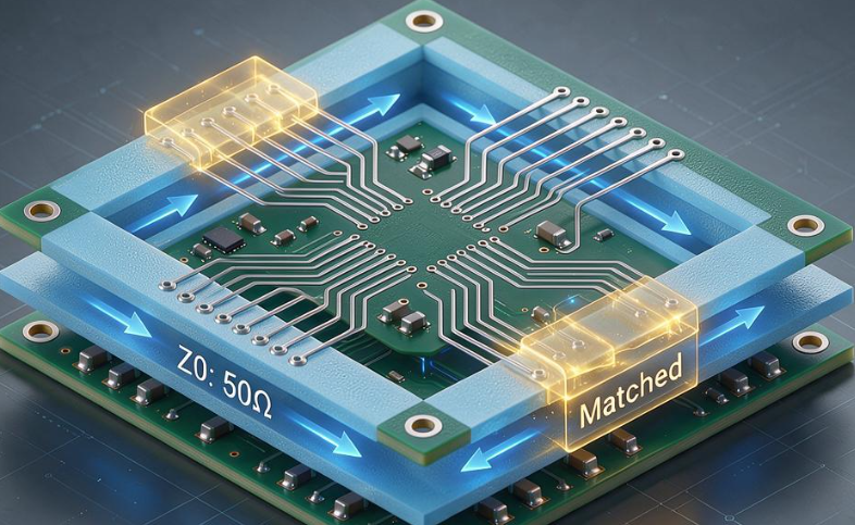
Consider a nominal 50 Ω transmission line. The design should not be evaluated only at the nominal dielectric thickness and nominal Dk.
Instead, engineers should consider combinations such as:
- Minimum dielectric thickness + maximum effective Dk → lower impedance tendency
- Maximum dielectric thickness + minimum effective Dk → higher impedance tendency
These combinations represent useful worst-case boundaries for preliminary analysis.
However, real manufacturing variation is not always perfectly correlated or statistically independent. Therefore, a worst-case calculation should be distinguished from a statistical tolerance analysis.
A simple worst-case approach is useful for establishing design margins, while a statistical approach can provide a more realistic estimate of production distribution when sufficient process data is available.
3. Build an Impedance Tolerance Budget
The total allowable impedance variation should be allocated among the major manufacturing variables during the early design stage.
For example, if a product specifies:
50 Ω ±10%
the allowable impedance range is approximately 45–55 Ω.
That tolerance should not be treated as a margin that can be consumed entirely by trace-width variation. The overall impedance variation may be influenced by:
- Dielectric Thickness
- Dielectric Constant (Dk)
- Copper thickness
- Trace width
- Trace etching
- Surface finish
- Registration and layer-to-layer alignment
- Stackup variation
- Manufacturing process variation
A practical impedance budget identifies how sensitive the target impedance is to each variable.
For example:
| Variable | Potential Effect on Impedance | DFM Consideration |
|---|---|---|
| Dielectric thickness | Changes trace-to-plane spacing | Control material and lamination |
| Dk | Changes effective electromagnetic properties | Use appropriate material data |
| Trace width | Directly affects impedance | Define fabrication tolerance |
| Copper thickness | Changes conductor geometry | Control finished copper |
| Etching | Changes final trace width | Review process capability |
| Stackup variation | Changes transmission-line geometry | Validate actual stackup |
| Surface finish | Can slightly affect geometry/electrical behavior | Consider for critical designs |
If dielectric variation consumes most of the available impedance margin, there may be insufficient tolerance left for normal fabrication variation.
In that situation, simply tightening the trace-width requirement may not solve the underlying problem. A better approach may be to select materials with tighter relevant tolerances, modify the stackup, or redesign the transmission-line geometry to provide greater manufacturing margin.
4. Reduce Sensitivity Through PCB Stackup Design
The PCB Stackup itself can be optimized to reduce impedance sensitivity.
When the dielectric layer between a trace and its reference plane is very thin, a relatively small change in dielectric thickness can produce a more noticeable percentage change in the transmission-line geometry.
Where mechanical and electrical requirements permit, increasing the dielectric spacing can sometimes reduce the relative sensitivity of impedance to small thickness variations.
However, increasing dielectric thickness is not automatically the best solution. It may affect:
- Overall PCB thickness
- Layer count and construction
- Via aspect ratio
- Signal propagation
- Crosstalk
- EMI behavior
- Controlled-impedance geometry
- Manufacturing cost
The stackup should therefore be optimized as a complete electrical and manufacturing system.
5. Minimize Unnecessary Prepreg Combinations
Prepreg construction is another important consideration in PCB Stackup design.
When multiple prepreg sheets are combined to form a dielectric layer, the final thickness depends on the characteristics and resin flow of each sheet. Multiple material tolerances can also contribute to overall variation.
Where the required dielectric thickness and lamination process allow it, simplifying the prepreg construction can reduce unnecessary sources of variation.
However, using fewer prepreg sheets is not a universal rule. Resin requirements, copper pattern, glass style, lamination performance, mechanical requirements, and target dielectric thickness must all be considered.
The objective should be a stackup that provides predictable post-lamination thickness and stable electrical performance.
6. Consider Copper Distribution During Lamination
Dielectric thickness is not determined by material specifications alone.
Copper distribution has a significant influence on resin flow during multilayer lamination. Areas with different copper densities can experience different resin-flow behavior, potentially resulting in local variation in the final dielectric thickness.
This is particularly important when impedance-controlled traces are located in regions with substantially different copper patterns from the surrounding PCB.
Designers should therefore review:
- Copper density across layers
- Large copper-free regions
- Large isolated copper areas
- Reference-plane openings
- Copper balancing requirements
- Panelization effects
Maintaining a more balanced copper distribution can help make the lamination process more predictable.
For high-speed transmission lines, reference planes should also remain continuous wherever possible. Unnecessary plane voids beneath controlled-impedance traces can alter the return-current path and change the effective transmission-line structure.
7. Material Selection Should Include Tolerance Data
Selecting a laminate based only on its nominal Dk value is insufficient for demanding Impedance Control applications.
Before finalizing the material system, engineers should review the available technical data, including:
- Nominal Dk
- Dk measurement frequency
- Df
- Thickness tolerance
- Resin content
- Glass style
- Thermal properties
- Lot-to-lot variation where available
- Recommended fabrication conditions
For high-speed applications, material characterization data should be appropriate for the actual frequency range.
If the design requires especially tight impedance control, communication between the PCB designer, material supplier, and fabricator becomes important. The simulation model should represent the material system that will actually be manufactured.
8. Control Materials During Mass Production
Once a design enters production, material incoming inspection becomes an important part of impedance control.
Before production, engineers should verify the specified core and prepreg materials against the approved stackup.
For higher-reliability or tighter-tolerance applications, manufacturers may also establish lot-level material verification requirements based on the product specification and supplier documentation.
Relevant incoming information can include:
- Material identification
- Core thickness
- Prepreg specification
- Resin content
- Dk/Df data where available
- Supplier lot information
- Certificate of conformity or material report
Not every PCB requires direct Dk measurement for every incoming lot. The appropriate verification method should be based on the required impedance tolerance, material system, supplier controls, and quality plan.
9. Use TDR Testing to Validate Production Impedance
TDR Testing (Time-Domain Reflectometry) is commonly used to evaluate controlled impedance on manufactured PCBs.
A properly designed impedance coupon can provide a practical way to verify whether the fabricated board meets the specified impedance requirements.
The test structure should represent the actual transmission-line configuration as closely as possible, including:
- Signal layer
- Reference-plane arrangement
- Dielectric construction
- Trace width
- Copper thickness
- Relevant surface-finish conditions
The test method, calibration requirements, coupon design, measurement location, and acceptance criteria should be defined in advance.
For production control, sampling frequency should follow the customer’s quality requirements and agreed inspection plan. AQL may be appropriate in some production environments, but it should not be treated as a universal requirement for every impedance-controlled PCB.
10. Evaluate Board-to-Board and Within-Board Variation
Impedance consistency has two dimensions:
Within-board variation: impedance changes between different areas of the same PCB.
Board-to-board variation: impedance changes between individual PCBs produced in the same or different production lots.
Both should be considered when investigating production instability.
A standard coupon can provide valuable production information, but it may not capture every local variation on the product itself. For demanding designs, engineers may use additional test structures or carefully selected measurement locations to investigate possible regional differences.
If significant impedance dispersion is observed, the investigation should consider several factors rather than assuming that trace etching is the only cause.
A useful troubleshooting sequence is:
- Verify the material lot and material specifications.
- Check actual core and post-lamination dielectric thickness.
- Review lamination process stability.
- Verify copper thickness and trace geometry.
- Confirm the stackup used in production.
- Review the impedance coupon design.
- Check TDR calibration and measurement conditions.
- Compare measured data with the simulation model.
This systematic approach makes it easier to identify the dominant source of variation.
11. Statistical Tolerance Analysis for High-Precision Designs
For particularly demanding impedance-controlled products, a statistical approach can complement traditional worst-case analysis.
Instead of assuming that every variable simultaneously reaches its extreme value, engineers can use historical manufacturing data to estimate the actual distribution of:
- Dielectric thickness
- Dk
- Copper thickness
- Trace width
- Etching variation
- Lamination variation
This information can then be incorporated into a statistical impedance model.
The result can help engineers estimate the expected impedance distribution and determine whether the process has sufficient capability margin.
However, statistical analysis is only as reliable as the underlying manufacturing data. If the process data is limited or inconsistent, worst-case engineering analysis remains an important design tool.
12. Common Mistakes in Dielectric Tolerance Analysis
Several common practices can increase the risk of impedance problems during mass production.
| Mistake | Risk | Recommended Approach |
|---|---|---|
| Using only nominal Dk | Simulation may not represent production | Review relevant Dk data and variation |
| Ignoring dielectric thickness tolerance | Impedance may shift after lamination | Include thickness tolerance in analysis |
| Allocating all tolerance to trace width | Little margin remains for material variation | Establish a complete impedance budget |
| Using an oversimplified stackup model | Simulation-to-production mismatch | Model the actual material construction |
| Ignoring copper distribution | Local dielectric thickness may vary | Perform copper-balance review |
| Using an unrepresentative coupon | TDR results may not reflect product traces | Match coupon and product structures |
| Tightening trace width unnecessarily | Manufacturing difficulty increases | First identify the dominant sensitivity |
| Changing materials without re-simulation | Electrical characteristics may change | Revalidate the stackup and impedance |
13. A Practical PCB Dielectric Tolerance Workflow
A complete PCB Dielectric Tolerance workflow can be organized into the following stages:
- Define the required impedance targets and tolerances.
- Establish the PCB Stackup.
- Select suitable dielectric materials.
- Collect relevant Dk and thickness data.
- Calculate nominal impedance.
- Perform sensitivity analysis.
- Evaluate worst-case combinations.
- Allocate the impedance tolerance budget.
- Optimize trace geometry and stackup margin.
- Review copper distribution and lamination risks.
- Define material and manufacturing requirements.
- Validate impedance during prototype production.
- Monitor production material and process variation.
- Perform TDR Testing according to the agreed quality plan.
- Compare production data with simulation and update the model when necessary.
This workflow moves impedance control from a one-time simulation activity to a continuous design-and-manufacturing process.

14. Kingda PCB Impedance and Dielectric DFM Support
Kingda can support customers with multilayer PCB design and manufacturing reviews focused on Impedance Control, material selection, stackup construction, manufacturability, and production validation.
For impedance-sensitive designs, the engineering review can consider the relationship between dielectric thickness, Dielectric Constant (Dk), copper geometry, PCB Stackup, and manufacturing tolerances.
By identifying dielectric-related risks before production and validating the manufactured structure through appropriate testing, engineers can establish greater process margin and reduce the probability of impedance failures during volume production.
Conclusion
Stable impedance in mass-produced multilayer PCBs cannot be achieved by optimizing trace width alone. PCB Dielectric Tolerance, dielectric thickness, Dielectric Constant (Dk), copper geometry, lamination behavior, and stackup construction all contribute to the final impedance distribution.
The key is to move beyond nominal impedance simulation and establish a complete tolerance budget. By combining worst-case analysis, sensitivity evaluation, material control, optimized PCB Stackup design, and appropriate TDR Testing, engineers can identify impedance risks before they become production problems.
For high-speed and tightly controlled-impedance PCBs, incorporating dielectric tolerance analysis into the DFM process provides a practical foundation for improving batch-to-batch consistency, reducing rework, and supporting stable mass production.