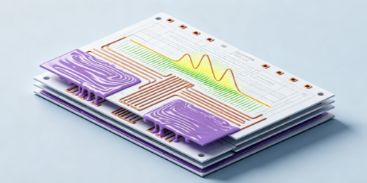
In multilayer PCB manufacturing, engineers usually calculate impedance based on trace width, copper thickness, dielectric thickness, and dielectric constant. However, the actual pressed structure can differ from the nominal stackup because prepreg resin flow changes the final dielectric thickness during lamination.
This is especially important for impedance-controlled and high-speed PCBs. If resin flows excessively into copper gaps or around large copper features, the final distance between the signal trace and its reference plane may become different from the value used in the original simulation.
The result can be an impedance shift even when the original stackup calculation is correct.
Understanding prepreg resin flow is therefore essential for maintaining stable impedance control from PCB design through mass production.
Why Prepreg Resin Flow Changes Dielectric Thickness
Prepreg is a composite material consisting primarily of glass reinforcement and resin. Before lamination, its nominal thickness does not necessarily represent the final dielectric thickness inside a finished multilayer PCB.
During lamination, the resin softens and flows under heat and pressure. It fills spaces around copper patterns and bonds the layers together.
The amount of resin movement depends on factors such as:
- Resin content
- Glass-weave construction
- Copper pattern density
- Copper thickness
- Copper surface profile
- Lamination temperature
- Pressing pressure
- Heating and cooling rate
- Lamination cycle
- Stackup construction
As resin moves during pressing, the final dielectric thickness can change locally.
For a transmission line, the distance between the signal conductor and its reference plane is a critical parameter. A change in this distance changes the electromagnetic field distribution and therefore affects characteristic impedance.
The relationship can be represented conceptually as:
[Z_0=f(W,T,H,D_k)]
where:
- (W) is trace width
- (T) is copper thickness
- (H) is dielectric spacing
- (D_k) is the effective dielectric constant
The equation is a simplified representation rather than a universal impedance formula. Actual impedance must be calculated according to the specific microstrip, stripline, or other transmission-line geometry.
Copper Pattern Density Controls Where Resin Flows
One of the most important factors affecting prepreg resin flow is copper distribution.
A multilayer PCB rarely has uniform copper density across its entire surface. Some regions may contain large copper planes, while others contain isolated traces or relatively open areas.
During lamination, resin tends to move toward regions where it can fill available spaces. The local copper pattern therefore affects the final resin distribution and dielectric thickness.
This creates a potential chain of effects:
Copper pattern → resin flow → pressed dielectric thickness → field distribution → impedance
This is why two locations on the same PCB can sometimes exhibit different electrical behavior even though they use the same prepreg material.
The effect becomes more important for fine-line, high-density, and tightly controlled impedance structures.
Resin Content and Resin Flow Are Different Parameters
A common mistake is to select prepreg based only on the material designation.
Two prepregs with similar nominal thickness can behave differently during lamination because their resin content and flow characteristics are different.
Resin content describes the proportion of resin within the prepreg construction.
Resin flow describes how the resin behaves under specified processing conditions.
These parameters affect how the prepreg fills copper features and how much material remains around the finished copper structure.
However, there is no universal rule stating that higher resin content or lower resin flow is always better.
The correct selection depends on:
- Finished dielectric thickness
- Copper pattern density
- Required impedance
- Layer-to-layer spacing
- Board thickness
- Via structure
- Lamination capability
- Thermal requirements
- Manufacturing yield
For impedance-critical layers, the PCB manufacturer should provide validated pressed-thickness data rather than relying only on nominal prepreg specifications.
Why Nominal Prepreg Thickness Can Mislead Impedance Simulation
A stackup table may list a prepreg as having a nominal thickness of a few mils. This does not mean the finished dielectric layer will have exactly that thickness after lamination.
For example, a simulation may assume a dielectric thickness of 2.3 mil, while the actual pressed thickness is different because of resin flow and copper-pattern effects.
If the simulation uses only nominal data, the calculated impedance may not accurately represent the finished PCB.
This does not necessarily mean the simulation is incorrect.
The more likely issue is that the physical structure differs from the model.
A better workflow is:
Nominal stackup → lamination model → validated pressed thickness → impedance simulation → test coupon correlation
This approach helps reduce the gap between design assumptions and production results.
How Dielectric Thickness Influences Impedance
For many common transmission-line structures, increasing the distance between the signal trace and its reference plane changes the field distribution and characteristic impedance.
The exact direction and magnitude of the impedance change depend on the transmission-line geometry.
For example, in a common microstrip structure, the distance between the trace and reference plane is one of the major geometric variables. If the dielectric spacing changes while trace width and copper thickness remain unchanged, the resulting impedance will also change.
For a controlled-impedance design, this means that dielectric thickness should be treated as an electrical parameter rather than merely a mechanical dimension.
A useful engineering principle is:
Do not model the prepreg by nominal thickness alone. Model the pressed dielectric structure that the manufacturer can actually produce.
Thick Copper Makes Resin Flow More Difficult to Predict
Thick copper structures can make lamination more challenging because large copper features create significant height differences between copper and dielectric regions.
For example, an inner layer containing heavy copper traces or large copper planes may create local topography that changes how resin fills the surrounding space.
This can affect:
- Local dielectric thickness
- Resin distribution
- Glass-weave position
- Signal-to-plane spacing
- Impedance consistency
The effect is not limited to very thick copper. Even moderate copper-density differences can influence the final stackup when tight dimensional tolerances are required.
Therefore, copper thickness and copper pattern distribution should be considered during stackup development.
Prepreg Selection for Impedance-Controlled PCBs
For impedance-sensitive layers, engineers should evaluate prepreg based on actual lamination behavior rather than simply selecting a material with a familiar part number.
Important parameters include:
- Resin content
- Resin flow characteristics
- Glass style
- Final pressed thickness
- Effective Dk
- Df
- Copper thickness
- Copper pattern density
- Lamination process window
Different glass styles can produce different dielectric thicknesses after pressing even when their nominal dry thicknesses appear similar.
For this reason, PCB manufacturing capability should be considered at the beginning of stackup design.
A Practical Three-Step Control Method
1. Establish the Realistic Pressed Stackup
Before impedance simulation, define the expected post-lamination dielectric thickness.
The PCB manufacturer should provide construction data based on actual press capability, material combination, copper distribution, and historical production results.
The stackup should include:
- Core thickness
- Prepreg construction
- Target dielectric thickness
- Copper thickness
- Layer sequence
- Impedance targets
- Manufacturing tolerances
For high-speed designs, it is preferable to define a nominal value together with an acceptable process window rather than rely on one ideal dimension.
2. Correlate Cross-Section Measurements With Impedance
After lamination, cross-sectional analysis can determine whether the actual dielectric structure matches the design assumption.
Engineers can compare:
- Designed dielectric thickness
- Actual pressed thickness
- Copper thickness
- Trace width
- Reference-plane spacing
- TDR impedance results
This provides much stronger evidence than adjusting the trace width simply because the first impedance measurement is outside the target.
If the physical stackup is wrong, changing trace width may only compensate for one location while creating another mismatch elsewhere.
3. Include Manufacturing Tolerances in the Impedance Model
A production-ready impedance model should consider realistic variation in:
- Dielectric thickness
- Trace width
- Copper thickness
- Dk
- Etching
- Registration
- Resin distribution
Sensitivity analysis can identify which parameter has the greatest influence on impedance.
For example, if impedance is highly sensitive to dielectric spacing but relatively insensitive to a small copper-thickness change, lamination control should receive greater attention.
This is a more efficient approach to impedance control than attempting to tighten every manufacturing parameter equally.
Cross-Section and Microscopic Analysis
When unexpected impedance variation occurs, cross-section analysis is one of the most useful physical verification methods.
A polished cross-section can reveal:
- Actual dielectric thickness
- Copper thickness
- Resin distribution
- Glass-weave position
- Copper-to-resin interface
- Voids
- Delamination
- Local structural deformation
Higher-resolution microscopy can be used when the root cause involves resin distribution, copper surface morphology, or localized defects.
However, techniques such as SEM or EDX should be selected according to the suspected failure mechanism. Elemental analysis alone cannot directly prove that excessive resin flow caused a particular impedance shift.
Physical measurements should therefore be correlated with electrical results.
Common Misunderstandings About Prepreg Resin Flow
Misunderstanding 1: Nominal prepreg thickness equals finished dielectric thickness
It does not. The final thickness depends on lamination conditions and the surrounding copper structure.
Misunderstanding 2: Higher resin content always improves impedance consistency
Not necessarily. Material selection must consider final dielectric thickness, glass construction, copper density, and the manufacturer’s lamination window.
Misunderstanding 3: A correct stackup simulation guarantees a correct production impedance
Simulation accuracy depends on the accuracy of the physical inputs.
Misunderstanding 4: Finished board thickness directly represents signal-to-plane spacing
It does not. Total board thickness includes multiple dielectric and copper layers.
Misunderstanding 5: Trace-width adjustment can solve every impedance problem
If the root cause is local dielectric variation, trace-width compensation may not provide a stable solution across the entire panel.
High-Speed PCB Applications Require Tighter Correlation
As signaling speeds increase, transmission-line dimensions become increasingly important.
High-speed channels can be sensitive to small changes in:
- Dielectric thickness
- Dk
- Trace width
- Copper roughness
- Via geometry
- Reference-plane spacing
Impedance variation can contribute to reflections, return loss, insertion-loss changes, inter-symbol interference, and eye-diagram degradation.
However, there is no universal frequency above which prepreg flow suddenly becomes a critical issue. Sensitivity depends on the complete channel, including rise time, channel length, stackup, impedance tolerance, and receiver requirements.
For this reason, high-speed PCB projects should use electrical validation together with physical stackup verification.
Recommended Checklist for Impedance-Controlled PCB Manufacturing
Before mass production, engineers can review the following items:
- Confirm the actual pressed thickness of critical prepreg layers.
- Verify resin content and flow characteristics.
- Review copper pattern density on adjacent layers.
- Include copper thickness in the stackup model.
- Use realistic effective Dk values.
- Define acceptable dielectric-thickness tolerances.
- Correlate cross-section measurements with impedance testing.
- Use TDR or appropriate impedance test methods.
- Review impedance variation across multiple locations and production panels.
- Track lamination capability and process stability over time.
- Revalidate the stackup when changing prepreg, copper distribution, or lamination conditions.
How Kingda Supports Impedance-Controlled PCB Manufacturing
Reliable PCB manufacturing requires close coordination between stackup engineering, prepreg selection, lamination, copper processing, and electrical testing.
Kingda can support impedance-controlled multilayer PCB projects by coordinating material selection, stackup development, lamination processes, impedance calculations, test coupons, and production verification.
By correlating actual pressed dielectric thickness with impedance measurements, engineers can identify whether a deviation originates from resin flow, copper geometry, etching, material variation, or another manufacturing factor.
This approach helps create a more stable transition from PCB design to prototype and mass production.
Conclusion
Prepreg resin flow is an important but sometimes overlooked factor in multilayer PCB impedance control.
During lamination, resin movement changes the final dielectric structure around copper features. Variations in resin content, glass construction, copper pattern density, copper thickness, and pressing conditions can therefore change the actual signal-to-reference-plane spacing.
The key is not to assume that nominal prepreg thickness represents the finished PCB.
For impedance-critical PCB design, the most reliable approach is to combine realistic pressed-stackup data, material characterization, manufacturing tolerances, cross-sectional analysis, and electrical verification.
When the physical stackup and impedance model are properly correlated, engineers can reduce unexpected impedance shifts and improve consistency across production panels and manufacturing lots.