Large-area copper voids in a PCB ground plane may appear to save material, reduce capacitance, improve manufacturability, or accommodate thermal and mechanical requirements. However, in high-speed and RF designs, excessive voiding can significantly change the electrical behavior of the reference structure.
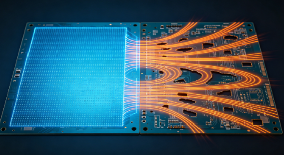
A continuous ground plane provides a low-impedance return path and helps contain electromagnetic fields. When the plane is replaced by a large grid or extensive copper openings, the return current may be forced to detour around the gaps. This can increase loop inductance, create impedance discontinuities, and increase the potential for common-mode conversion and electromagnetic radiation.
For RF modules and other EMI-sensitive products, ground plane integrity should therefore be treated as both a signal-integrity and electromagnetic-compatibility requirement.
How Ground Plane Discontinuities Affect High-Frequency Return Current
At high frequencies, return current tends to concentrate in the region of the reference plane close to the signal conductor. The exact distribution depends on the stackup, dielectric thickness, trace geometry, frequency, and field configuration.
When a continuous ground plane is replaced by a large-area grid, the return path may no longer remain directly beneath the signal trace.
Instead, current must flow around openings or pass through alternative paths using vias and adjacent planes.
This increases the effective current-loop area and can increase inductance.
A simplified relationship is:
V = L × di/dt
where L is loop inductance and di/dt represents the rate of current change.
As loop inductance increases, high-speed current transients can produce larger voltage disturbances. In an RF or high-speed PCB, this can contribute to:
- Impedance discontinuity
- Return-path detours
- Increased common-mode current
- Crosstalk
- Ground noise
- Electromagnetic radiation
- EMI/EMC degradation
Therefore, a ground plane should not be evaluated simply by its percentage of copper coverage. The return path and electromagnetic field distribution are more important than copper percentage alone.
Why Large Ground Voids Can Increase EMI
A large opening in a reference plane does not automatically behave as an antenna. However, depending on its dimensions, geometry, location, and surrounding structure, it can become an efficient electromagnetic coupling path.
The relevant dimensions should be compared with the wavelength associated with the signal’s significant frequency content.
The free-space wavelength can be approximated as:
λ = c / f
where c is the speed of light and f is frequency.
For example, the free-space wavelength at 3.5 GHz is approximately 85.7 mm. However, PCB structures do not behave exactly like free-space structures because the effective wavelength is affected by the dielectric environment and electromagnetic boundary conditions.
Therefore, using a universal rule such as “any opening larger than λ/20 will resonate” is an oversimplification.
A more reliable evaluation considers:
- Opening length and width
- Effective dielectric constant
- Plane-to-plane spacing
- Signal frequency and edge rate
- Ground-plane geometry
- Cavity dimensions
- Via placement
- Enclosure structure
- Location relative to RF traces and components
Large, regularly repeated openings can also create periodic electromagnetic structures. Under certain conditions, these structures may support resonant modes or increase coupling at specific frequencies.
Ground Plane Integrity Is More Important Than Copper Fill Percentage
One common design mistake is to judge a ground plane according to its overall copper percentage.
For example, a 70% copper-filled plane may appear electrically adequate when viewed from a CAD layout. However, if the remaining 30% consists of large openings located directly beneath sensitive RF traces, connectors, or high-speed differential pairs, the electrical impact may be much greater than the percentage suggests.
Conversely, a plane with a lower overall copper percentage may perform acceptably if the remaining copper provides a continuous, low-inductance return path around critical circuits.
Therefore, PCB grounding should be evaluated based on electrical continuity and current distribution rather than simply the amount of copper remaining.
Large Voids Can Distort the Reference Plane
A reference plane serves more than one purpose.
It provides:
- A return-current path
- A controlled electromagnetic reference
- A low-impedance connection between circuit regions
- A shielding structure
- A reference for controlled-impedance traces
When a large void is introduced, these functions can be affected simultaneously.
For controlled-impedance traces, the trace impedance depends on conductor width, copper thickness, dielectric thickness, dielectric properties, and the surrounding electromagnetic geometry.
If the distance between the trace and its reference plane changes locally, the characteristic impedance may also change.
As a result, a large ground opening beneath a high-speed or RF trace can create a local impedance discontinuity.
The effect becomes more significant when the discontinuity is electrically long relative to the signal’s rise time or relevant frequency spectrum.
Ground Plane Voids and Common-Mode Conversion
Differential signaling is often considered inherently resistant to electromagnetic interference. However, a differential pair still requires a well-controlled electromagnetic environment.
If one side of a differential pair encounters a different reference-plane geometry from the other side, the two conductors may experience different return-path conditions.
This asymmetry can convert part of the differential signal into common-mode energy.
Common-mode current is particularly important in EMI analysis because it can travel through cables, connectors, chassis structures, and other conductive paths and become a significant radiation source.
Therefore, EMI shielding cannot be evaluated independently from signal routing and reference-plane continuity.
For high-speed differential interfaces, engineers should check:
- Reference-plane continuity
- Pair symmetry
- Via transitions
- Connector transitions
- Ground stitching
- Plane openings
- Differential impedance
- Common-mode conversion
Why RF PCBs Are Particularly Sensitive
RF circuits often operate with relatively small electromagnetic wavelengths and tightly controlled impedance environments.
At several gigahertz, even a relatively small PCB structure can become electrically significant.
This is why RF PCB design requires careful coordination between:
- Transmission lines
- Ground planes
- Via fences
- Component placement
- Connector transitions
- Shielding structures
- Ground stitching
- PCB enclosure interfaces
A large ground-plane opening near an RF transmission line can change the local electromagnetic field and increase coupling.
However, the effect cannot be predicted from opening size alone. Full-stackup electromagnetic simulation or measurement is often necessary for demanding RF designs.
Copper Thickness Does Not Directly Determine Shielding Performance
Another common misunderstanding is that thicker ground copper automatically provides substantially better shielding.
Copper thickness affects sheet resistance and current distribution, but once the copper is sufficiently conductive at the operating frequency, the geometry and continuity of the ground structure often become more important.
For many PCB applications, the primary concern is therefore not simply whether the ground copper is 0.5 oz, 1 oz, or 2 oz.
Engineers should instead evaluate:
- Plane continuity
- Return-path inductance
- Ground via density
- Plane-to-plane spacing
- Current distribution
- Surface current
- Trace-to-plane geometry
- Frequency-dependent behavior
A thin but continuous ground plane can perform better electrically than a thick plane with large discontinuities.
Ground Grid Design Requires Careful Geometry Control
Ground grids are sometimes used for thermal, mechanical, manufacturing, or other design reasons. They are not inherently unsuitable for every application.
The key question is where the grid is located and what function the plane performs.
A grid may be acceptable in a low-frequency or non-critical region while being inappropriate directly underneath an RF transmission line or high-speed interface.
If openings are necessary, consider:
- Reducing individual opening dimensions
- Avoiding long continuous slots
- Keeping critical signal paths over continuous copper
- Staggering openings where appropriate
- Maintaining adequate ground stitching
- Avoiding symmetrical structures that unintentionally reinforce resonant behavior
- Checking the grid against the actual operating spectrum
There is no universal maximum opening dimension that applies to every PCB.
The acceptable geometry depends on the stackup and electromagnetic requirements.
Do Not Confuse a Reference Plane With a Dedicated Shielding Layer
In a multilayer PCB, the ground plane can simultaneously function as a signal reference and contribute to electromagnetic containment.
However, these functions are not always identical.
A ground plane beneath a microstrip or stripline primarily provides an electrical reference and return path. A dedicated shielding layer, enclosure, via fence, or conductive cavity may perform additional electromagnetic-containment functions.
Therefore, removing copper from a signal reference plane can affect signal integrity even if another copper layer exists elsewhere in the PCB.
For this reason, engineers should analyze the complete three-dimensional current path rather than assuming that another ground layer automatically compensates for the discontinuity.
Common Design Mistakes
Mistake 1: Using Copper Percentage as the Main Criterion
A large percentage of copper does not guarantee a low-impedance return path.
The location and shape of the remaining copper are more important.
Mistake 2: Putting Large Voids Under High-Speed Traces
A large opening directly beneath a critical signal can force the return current to detour.
This can increase loop area and create local impedance and EMI problems.
Mistake 3: Creating Long, Continuous Slots
A long slot can behave differently from a collection of small isolated openings.
Its electrical length and orientation relative to nearby traces can make it more significant at particular frequencies.
Mistake 4: Ignoring Via Transitions
A signal that changes layers may also require its return current to transition between reference planes.
A nearby ground stitching via can provide a lower-inductance return path and reduce unnecessary current spreading.
Mistake 5: Validating Only With DC Measurements
DC resistance measurements cannot fully characterize RF or high-speed ground-plane performance.
For demanding designs, frequency-domain measurements and electromagnetic simulation are more appropriate.
A Better Validation Method for EMI-Sensitive PCBs
For an EMI-critical board, the effect of ground-plane openings should be verified through a combination of simulation and measurement.
A practical workflow includes:
Step 1: Review the stackup
Determine the dielectric thickness, reference-plane locations, copper thickness, and controlled-impedance structures.
Step 2: Map critical signal paths
Identify RF transmission lines, high-speed differential pairs, clock signals, switching nodes, and sensitive analog circuits.
Step 3: Check the reference plane
Inspect whether any slots, voids, thermal reliefs, or grid structures intersect the expected return-current region.
Step 4: Review ground stitching
Check the placement of ground vias around RF circuits, connectors, board edges, and shielding boundaries.
Step 5: Perform electromagnetic simulation
For demanding applications, use a suitable 2D or 3D electromagnetic solver to evaluate current distribution, impedance, coupling, and resonant behavior.
Step 6: Conduct prototype measurements
Depending on the design objective, measurements may include:
- S-parameters
- TDR impedance
- Near-field scanning
- Radiated-emission testing
- Conducted-emission testing
- Shielding-effectiveness testing
A VNA measurement such as S21 can characterize transmission or coupling between defined ports, but it should not be automatically interpreted as a direct measurement of PCB shielding effectiveness. The fixture, port configuration, calibration, sample geometry, and test method determine what the measured S21 actually represents.

How Kingda Approaches Ground Plane Optimization
At Kingda, ground-plane optimization is evaluated as part of the complete PCB design and manufacturing process rather than by applying a single copper-fill rule.
For EMI-sensitive and RF products, the review can include:
- Stackup analysis
- Reference-plane continuity
- Controlled-impedance routing
- Ground-via placement
- Copper-opening geometry
- RF transmission-line layout
- Differential-pair return paths
- Manufacturing tolerances
- Prototype EMI validation
If a copper opening is required for thermal or mechanical reasons, the design should be analyzed based on its actual electrical location and operating frequency.
The objective is not necessarily to eliminate every copper void. It is to ensure that unavoidable openings do not compromise critical return paths or create unacceptable electromagnetic coupling.
Conclusion
Large copper openings in a PCB ground plane can affect both PCB grounding and electromagnetic behavior by disturbing return-current paths, increasing loop inductance, creating local impedance discontinuities, and potentially increasing common-mode radiation.
The impact depends on much more than the percentage of copper removed. Opening geometry, electrical length, stackup, dielectric thickness, signal rise time, operating frequency, ground stitching, and surrounding structures all influence the result.
For high-speed and RF applications, maintaining ground plane integrity beneath critical signal paths is usually more important than maximizing or minimizing copper fill as a single design target.
With appropriate RF PCB design, return-path analysis, electromagnetic simulation, and prototype EMI testing, engineers can determine where copper openings are acceptable and where continuous copper should be preserved.
Kingda can support this process by coordinating PCB stackup, grounding, impedance control, manufacturing capability, and reliability validation from design through production.